
ICE40UP5K to PCM5102A, I2S out

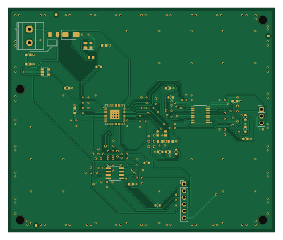
About the ICE40UP5K to PCM5102A, I2S out PCB
ICE40UP5K to PCM5102A, I2S out is an open source FPGA PCB design by sabas0ba, published on GitHub under the Apache-2.0 license. It is a 2-layer board measuring 100 × 84 mm, with 33 components from 16 distinct parts.
Its main chip is the ICE40UP5K-SG48ITR, from the FPGA family. Other key parts include the PCM5102APWR, AP2112K-1.2TRG1 and W25Q32JVSSIQ. By type, the board carries 17 capacitors, 6 resistors, 4 ICs, 3 connectors, 1 crystal and 1 fuse.
It belongs with the audio designs in this gallery.
From the project
Container-based toolkit for circuit design: datasheets, SPICE simulation and KiCad review
Each project here exists twice, generated from one description by tools/makeexamples.py`:
A repository full of good designs proves only that good designs pass. The pair is the evidence: that the rules catch what they claim to catch, and that fixing what they report converges.
Gate acceptance is not production sign-off. These are worked examples, not hardware-validated reference designs. In particular, the FPGA still has decoupling-distance exceptions; signal return paths, application-specific power/thermal budgets and EMC remain engineering review and measurement work.
Main components on the ICE40UP5K to PCM5102A, I2S out
ICE40UP5K to PCM5102A, I2S out bill of materials (BOM)
33 components, 16 distinct parts.
| Qty | Part | Footprint | Refs |
|---|---|---|---|
| 1 | ICE40UP5K-SG48ITR iCE40UP5K Lattice Semiconductor | QFN-48-1EP_7x7mm_P0.5mm_EP3.5x3.5mm | U1 |
| 1 | PCM5102APWR PCM5102A Texas Instruments | TSSOP-20_4.4x6.5mm_P0.65mm | U2 |
| 1 | AP2112K-1.2TRG1 AP2112K-1.2 Diodes Incorporated | SOT-23-5 | U3 |
| 1 | W25Q32JVSSIQ W25Q32JV Winbond | SOIC-8_3.9x4.9mm_P1.27mm | U4 |
| 1 | ASE-12.000MHZ-L-C-T 12MHz Abracon | Oscillator_SMD_Abracon_ASE-4Pin_3.2x2.5mm | X1 |
| 1 | 1729128 3V3 IN Phoenix Contact | TerminalBlock_Phoenix_MKDS-1,5-2_1x02_P5.00mm_Horizontal | J1 |
| 1 | 61300311121 AUDIO OUT Wurth Elektronik | PinHeader_1x03_P2.54mm_Vertical | J2 |
| 1 | 61300611121 SPI PROG Wurth Elektronik | PinHeader_1x06_P2.54mm_Vertical | J3 |
| 1 | 0466.500NR 500mA Littelfuse | Fuse_1206_3216Metric | F1 |
| 1 | SMAJ5.0A Littelfuse | D_SMA | D3 |
| 3 | CL10A106MQ8NNNC 10u Samsung | C_0603_1608Metric | C1, C3, C17 |
| 11 | CL10B104KB8NNNC 100n Samsung | C_0603_1608Metric | C2, C4, C5, C6, C7, C8, C9, C10 +3 |
| 3 | CL10A225KO8NNNC 2u2 Samsung | C_0603_1608Metric | C12, C13, C14 |
| 4 | RC0603FR-0710KL 10k Yageo | R_0603_1608Metric | R1, R2, R4, R6 |
| 1 | RC0603FR-07100RL 100R Yageo | R_0603_1608Metric | R3 |
| 1 | RC0603FR-0733RL 33R Yageo | R_0603_1608Metric | R5 |
ICE40UP5K to PCM5102A, I2S out design files
The KiCad project lives in the sabas0ba/kicad_skills repository on GitHub; these links point at the commit this page was built from.
ICE40UP5K to PCM5102A, I2S out: common questions
What microcontroller does the ICE40UP5K to PCM5102A, I2S out use?
The ICE40UP5K to PCM5102A, I2S out is built around the ICE40UP5K-SG48ITR, from the FPGA family.
How big is the ICE40UP5K to PCM5102A, I2S out PCB?
The ICE40UP5K to PCM5102A, I2S out measures 100 × 84 mm, has 2 copper layers and is 1.6 mm thick.
How many components are on the ICE40UP5K to PCM5102A, I2S out?
33 components, from 16 distinct parts. The full bill of materials is listed on this page.
Where can I download the ICE40UP5K to PCM5102A, I2S out design files?
From the sabas0ba/kicad_skills repository on GitHub, which has the KiCad layout and the schematic; the links under Design files point to each one.
Can I use the ICE40UP5K to PCM5102A, I2S out design in my own project?
Yes, under the terms of its Apache-2.0 license, which sabas0ba chose for the repository.
Can I test firmware for the ICE40UP5K to PCM5102A, I2S out without the hardware?
Yes. HardLabs builds a simulation of the board from its netlist and BOM, so you can run and debug FPGA firmware against it before you order a PCB.
More boards in kicad_skills
1 kHz Sallen-Key low pass, single 5 V
54 × 38 mm22 parts2LApache-2.01
Dual H-bridge, DRV8833PW, 2 x 0.5 A RMS
68 × 46 mm13 parts2LApache-2.01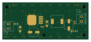
12 V to 5 V buck converter, 2 A
88 × 38 mm13 parts2LApache-2.01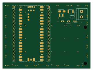 RP2040/RP2350
Raspberry Pi Pico carrier, 5 V in
80 × 60 mm10 parts2LApache-2.01
Similar boards
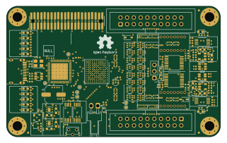 FPGA
Base board
GlasgowEmbedded
80 × 49 mm222 parts4L0BSD2.2k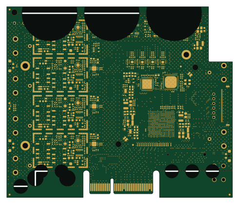 FPGA
Thunderscope Rev5.3
EEVengers
122.5 × 103.5 mm817 parts6LMIT1.3k FPGA
Usb sniffer
ataradov
58.2 × 38.1 mm86 parts2LBSD-3-Clause1.3k FPGA
Tomu, I'm
theacodes
13 × 9.4 mm40 parts4LMIT1.1k FPGA
Icepi zero
cheyao
65 × 30 mm143 parts4LSHL-2.1828 FPGA
Gcvideo
ikorb
49 × 30 mm44 parts4LNo license765