
Node pad v1

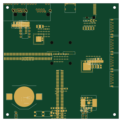
About the Node pad v1 PCB
Node pad v1 is an open source Raspberry Pi PCB design by Sami9889, published on GitHub under the CERN-OHL-P-2.0 license. It is a 4-layer board measuring 100 × 100 mm, with 209 components from 59 distinct parts.
Its main chip is the DF40C-100DS-0.4V, from the Raspberry Pi family. Other key parts include the RTL8125BG, MP2315GJ, AP2112K-3.3, CH224K and MP8007GV. By type, the board carries 14 connectors, 12 capacitors, 11 ICs, 7 resistors, 6 diodes and 2 switches.
It belongs with the power & battery and dev boards & breakouts designs in this gallery.
From the project
Status: Rev 0.1 placement/connectivity audit in progress — not fabrication-ready; do not order. See VERIFICATION.md for blocking footprint and pin-mapping defects. Author: Samrath "Sami" Singh License: TBD (MIT or CERN-OHL-P recommended if you plan to sell it)
Status: Rev 0.1 placement/connectivity audit in progress — not fabrication-ready; do not order. See VERIFICATION.md for blocking footprint and pin-mapping defects. Author: Samrath "Sami" Singh License: TBD (MIT or CERN-OHL-P recommended if you plan to sell it)
A carrier board for the Radxa CM5 compute module. You skip designing the CPU/RAM/eMMC section (Radxa already did that) and get a compact server-class SBC with I/O aimed at self-hosting, homelab, mini-Kubernetes, edge servers, network appliances, and NAS-lite.
Main components on the Node pad v1
Node pad v1 bill of materials (BOM)
209 components, 59 distinct parts — part numbers from the project's BOM.
| Qty | Part | Footprint | Refs |
|---|---|---|---|
| 1 | RTL8125BG | QFN-64-1EP_9x9mm_P0.5mm_EP4.7x4.7mm | U2 |
| 1 | MP2315GJ MP2315 | SOT-563 | U3 |
| 1 | AP2112K-3.3 | SOT-23-5 | U4 |
| 1 | CH224K | VSSOP-10_3x3mm_P0.5mm | U5 |
| 1 | MP8007GV MP8007 DNP | SOIC-16_3.9x9.9mm_P1.27mm | U6 |
| 1 | DS3231MZ+ | SOIC-8_3.9x4.9mm_P1.27mm | U7 |
| 1 | GL3523 | ArtInChip_QFN-88-1EP_10x10mm_P0.4mm_EP6.74x6.74mm | U10 |
| 4 | TPS2553DBVR TPS2553 | SOT-23-6 | U11, U12, U13, U14 |
| 1 | C1804 25MHz TCXO | Crystal_SMD_3225-4Pin_3.2x2.5mm | Y1 |
| 1 | DF40C-100DS-0.4V CM5-J1 | Hirose_BM24_BM24-40DS-2-0.35V_2x20_P0.35mm_PowerPin2_Vertical | J1 |
| 1 | DF40C-100DS-0.4V CM5-J2 | Hirose_BM24_BM24-40DS-2-0.35V_2x20_P0.35mm_PowerPin2_Vertical | J2 |
| 2 | 0826-1G1T-04-F RJ45 | RJ45_Amphenol_RJHSE538X-02 | J3, J4 |
| 1 | M.2_M-KEY_2280 M.2 M-key 2280 | PinHeader_2x38_P1.27mm_Vertical_SMD | J5 |
| 1 | M.2_E-KEY_2230 M.2 E-key 2230 | PinHeader_2x38_P1.27mm_Vertical_SMD | J6 |
| 1 | C165948 USB-C | USB_C_Receptacle_HRO_TYPE-C-31-M-12 | J7 |
| 4 | USB_A_3.0 USB3-A | USB3_A_Molex_48393-001 | J8, J9, J10, J11 |
| 1 | C2681 HDMI | HDMI_A_Molex_208658-1001_Horizontal | J12 |
| 1 | PINHEADER_2X20 GPIO40 | PinHeader_2x20_P2.54mm_Vertical | J13 |
| 1 | PINHEADER_1X04 Fan | PinHeader_1x04_P2.54mm_Vertical | J15 |
| 1 | BS-14-2500 CR2032 | BatteryHolder_Keystone_3002_1x2032 | BT1 |
Show 39 more
| Qty | Part | Footprint | Refs |
|---|---|---|---|
| 11 | 10uF | C_0805_2012Metric | C_AVDD_BULK_1, C_AVDD_BULK_2, C_AVDD_BULK_3, C_AVDD_BULK_4, C_BLK_3V3_AUX_01, C_BLK_3V3_AUX_02, C_BLK_3V3_AUX_03, C_BLK_5V_01 +3 |
| 59 | 100nF | C_0402_1005Metric | C_AVDD_HF_1, C_AVDD_HF_2, C_AVDD_HF_3, C_AVDD_HF_4, C_BAT_1, C_CM5_HF_1, C_CM5_HF_2, C_CM5_HF_3 +51 |
| 2 | 1nF/2kV | C_1210_3225Metric | C_BS_J3, C_BS_J4 |
| 7 | 10uF | C_0603_1608Metric | C_CM5_BULK_1, C_CM5_BULK_2, C_CM5_BULK_3, C_CM5_BULK_4, C_CM5_BULK_5, C_CM5_BULK_6, C_M2E_BULK |
| 1 | 22uF/6.3V | C_0805_2012Metric | C_M2M_BULK |
| 1 | 1uF | C_0402_1005Metric | C_RTC_2 |
| 4 | 150uF/6.3V | C_1206_3216Metric | C_VB_J8, C_VB_J9, C_VB_J10, C_VB_J11 |
| 2 | ESD5Z5.0 | D_SOD-523 | D_HDMI_CTL_1, D_HDMI_CTL_2 |
| 4 | HD01-T DNP | D_SMB | D_POE_1, D_POE_2, D_POE_3, D_POE_4 |
| 4 | SMBJ5.0A | D_SMB | D_TVS_J8, D_TVS_J9, D_TVS_J10, D_TVS_J11 |
| 5 | 600R@100MHz | L_0603_1608Metric | FB_AVDD_1, FB_AVDD_2, FB_AVDD_3, FB_AVDD_4, FB_HDMI_5V |
| 2 | BSS138 | SOT-23 | Q_DDC_1, Q_DDC_2 |
| 14 | 10k | R_0402_1005Metric | R_BOOT0_PU, R_BOOT1_PU, R_BOOT2_PU, R_DDC_G_1, R_DDC_G_2, R_DDC_HI_1, R_DDC_HI_2, R_DDC_LO_1 +6 |
| 16 | 75 | R_0402_1005Metric | R_BS_J3_1, R_BS_J3_2, R_BS_J3_3, R_BS_J3_4, R_BS_J3_5, R_BS_J3_6, R_BS_J3_7, R_BS_J3_8 +8 |
| 5 | 1k | R_0402_1005Metric | R_D1, R_D2, R_D3, R_D4, R_D5 |
| 4 | 0/DNP | R_0402_1005Metric | R_E_OPT_1, R_E_OPT_2, R_E_OPT_3, R_E_OPT_4 |
| 2 | 4.7k | R_0402_1005Metric | R_I2C1_SCL_PU, R_I2C1_SDA_PU |
| 4 | 30k | R_0402_1005Metric | R_ILIM_J8, R_ILIM_J9, R_ILIM_J10, R_ILIM_J11 |
| 2 | 49.9 DNP | R_0402_1005Metric | R_PCIE0_TERM_N, R_PCIE0_TERM_P |
| 1 | K2-1114ST-A4SW-06 RESET | SW_SPST_TL3305A | SW1 |
| 1 | K2-1114ST-A4SW-06 BOOT | SW_SPST_TL3305A | SW2 |
| 1 | 750317847 750317847 DNP | DIP-8_W7.62mm | T1 |
| 4 | USBLC6-2SC6 | SOT-23-6 | U_HDMI_ESD_1, U_HDMI_ESD_2, U_HDMI_ESD_3, U_HDMI_ESD_4 |
| 1 | LED_0603_GREEN Green | LED_0603_1608Metric | D1 |
| 1 | LED_0603_BLUE Blue | LED_0603_1608Metric | D2 |
| 2 | LED_0603_YELLOW Yellow | LED_0603_1608Metric | D3, D4 |
| 1 | LED_0603_RED Red | LED_0603_1608Metric | D5 |
| 1 | SMBJ12A | D_SMB | D6 |
| 1 | C1046 4.7uH/3A | L_Bourns_SRR1208_12.7x12.7mm | L1 |
| 4 | C19702 1uF | C_0402_1005Metric | C1, C2, C15, C16 |
| 3 | C19702 22uF/25V | C_0805_2012Metric | C3, C10, C11 |
| 2 | C19702 100nF | C_0402_1005Metric | C4, C13 |
| 1 | C19702 2.2nF | C_0402_1005Metric | C5 |
| 1 | C19702 100pF | C_0402_1005Metric | C6 |
| 1 | C19702 10uF/16V | C_0402_1005Metric | C12 |
| 4 | C25804 10k | R_0402_1005Metric | R1, R2, R6, R7 |
| 1 | C25804 0 | R_0402_1005Metric | R3 |
| 1 | C25804 100k | R_0402_1005Metric | R4 |
| 1 | C25804 52.3k | R_0402_1005Metric | R5 |
Node pad v1 design files
The KiCad project lives in the Sami9889/Node-pad-v1 repository on GitHub; these links point at the commit this page was built from.
- LayoutPCB/NodePad.kicad_pcb
- SchematicPCB/NodePad.kicad_sch
- BOMBOM.csv
Node pad v1: common questions
What microcontroller does the Node pad v1 use?
The Node pad v1 is built around the DF40C-100DS-0.4V, from the Raspberry Pi family.
How big is the Node pad v1 PCB?
The Node pad v1 measures 100 × 100 mm, has 4 copper layers and is 1.6 mm thick.
How many components are on the Node pad v1?
209 components, from 59 distinct parts, with part numbers taken from the project's own BOM. The full bill of materials is listed on this page.
Where can I download the Node pad v1 design files?
From the Sami9889/Node-pad-v1 repository on GitHub, which has the KiCad layout, the schematic and the BOM; the links under Design files point to each one.
Can I use the Node pad v1 design in my own project?
Yes, under the terms of its CERN-OHL-P-2.0 license, which Sami9889 chose for the repository.
Can I test firmware for the Node pad v1 without the hardware?
Yes. HardLabs builds a simulation of the board from its netlist and BOM, so you can run and debug Raspberry Pi firmware against it before you order a PCB.
Similar boards
 Raspberry Pi
Open source rover
nasa-jpl
220 × 178 mm144 parts2LApache-2.09.7k Raspberry Pi
SPIRIT
SPIRIT-org
82 × 155 mm130 parts6LCERN-OHL-S-2.01.3k Raspberry Pi
CM5RevEng
schlae
55 × 40 mm417 parts10LNo license1.0k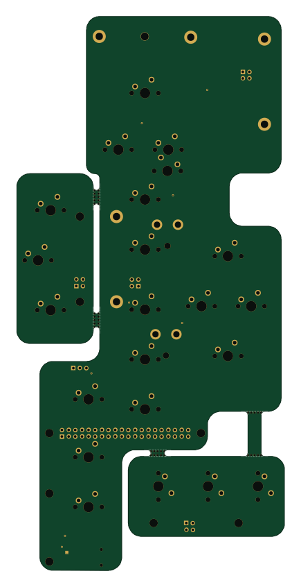 Raspberry Pi
Haxo hw
cardonabits
102.4 × 211.3 mm38 parts2LCustom license672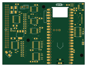 Raspberry Pi
PowerBook
BlueSCSI
74.5 × 56.3 mm78 parts2LGPL-3.0449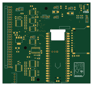 Raspberry Pi
Desktop 50 Pin TopConn
89.2 × 82.6 mm103 parts2LGPL-3.0449