
328p design

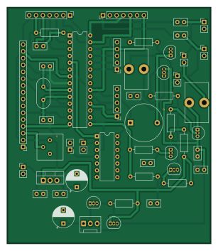
About the 328p design PCB
328p design is an open source AVR/Arduino PCB design by thesunRider, published on GitHub under the MIT license. It is a 2-layer board measuring 76 × 88 mm, with 51 components from 29 distinct parts.
Its main chip is the ATmega328-P, from the AVR/Arduino family. Other key parts include the TL431LP, 74HC04 and L7805. By type, the board carries 14 capacitors, 11 connectors, 9 resistors, 6 transistors, 4 ICs and 2 jumpers.
From the project
Lab Grade RF Generator (Square Wave) Made using Arduino and SI2302 Module
This is an open source DIY Square wave generator. There are two versions included: - Blue pill - (1Hz - 960Mhz) - Atmega328p/Arduino (1Hz - 250Mhz)
- Si5351 - Channel A,B (1Khz - 250Mhz) - CMT2119A - Channel E (only for bluepill version: 250Mhz - 960Mhz)
https://github.com/user-attachments/assets/bd40d5bd-5a4e-4a5a-9730-a542df9f6650
- Upload 328p schematics for an Arduino based generator. - Upload bluepill schematic for Bluepilll based generator.
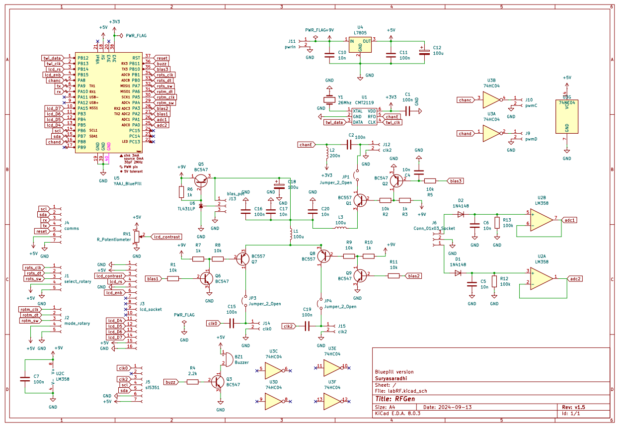
Main components on the 328p design
328p design bill of materials (BOM)
51 components, 29 distinct parts.
| Qty | Part | Footprint | Refs |
|---|---|---|---|
| 1 | ATmega328-P | DIP-28_W7.62mm | U1 |
| 1 | TL431LP | TO-92_Inline | U2 |
| 1 | 74HC04 | DIP-14_W7.62mm | U3 |
| 1 | L7805 | TO-220-3_Vertical | U4 |
| 4 | BC547 | TO-92_Inline | Q1, Q3, Q4, Q6 |
| 2 | BC557 | TO-92_Inline | Q2, Q5 |
| 1 | 20Mhz | Crystal_HC49-U_Vertical | Y1 |
| 1 | select_rotary | PinHeader_1x05_P2.54mm_Vertical | J1 |
| 1 | mode_rotary | PinHeader_1x05_P2.54mm_Vertical | J2 |
| 1 | lcd_socket | PinHeader_1x16_P2.54mm_Vertical | J3 |
| 1 | comms | PinHeader_1x07_P2.54mm_Vertical | J4 |
| 1 | si5351 | PinHeader_1x07_P2.54mm_Vertical | J5 |
| 1 | clk0 | PinHeader_1x02_P2.54mm_Vertical | J6 |
| 1 | clk2 | PinHeader_1x02_P2.54mm_Vertical | J7 |
| 1 | bias_pot | FanPinHeader_1x03_P2.54mm_Vertical | J8 |
| 1 | pwmD | PinHeader_1x02_P2.54mm_Vertical | J9 |
| 1 | pwmC | PinHeader_1x02_P2.54mm_Vertical | J10 |
| 1 | pwrIn | PinHeader_1x02_P2.54mm_Vertical | J11 |
| 1 | Buzzer | Buzzer_D14mm_H7mm_P10mm | BZ1 |
| 2 | Jumper_2_Open | PinHeader_1x02_P2.54mm_Vertical | JP1, JP2 |
Show 9 more
| Qty | Part | Footprint | Refs |
|---|---|---|---|
| 1 | R_Potentiometer | Potentiometer_Bourns_3386P_Vertical | RV1 |
| 2 | 100u | L_Toroid_Vertical_L14.7mm_W8.6mm_P5.58mm_Pulse_KM-1 | L1, L2 |
| 2 | 22p | C_Disc_D5.0mm_W2.5mm_P2.50mm | C1, C2 |
| 5 | 100n | C_Disc_D5.0mm_W2.5mm_P2.50mm | C3, C4, C5, C11, C13 |
| 5 | 10n | C_Disc_D5.0mm_W2.5mm_P2.50mm | C6, C7, C8, C10, C15 |
| 2 | 100u | CP_Radial_D8.0mm_P5.00mm | C12, C14 |
| 5 | 10k | R_Axial_DIN0207_L6.3mm_D2.5mm_P10.16mm_Horizontal | R1, R2, R6, R8, R10 |
| 1 | 2.2k | R_Axial_DIN0207_L6.3mm_D2.5mm_P10.16mm_Horizontal | R4 |
| 3 | 1k | R_Axial_DIN0207_L6.3mm_D2.5mm_P10.16mm_Horizontal | R5, R7, R9 |
328p design design files
The KiCad project lives in the thesunRider/RFGen repository on GitHub; these links point at the commit this page was built from.
328p design: common questions
What microcontroller does the 328p design use?
The 328p design is built around the ATmega328-P, from the AVR/Arduino family.
How big is the 328p design PCB?
The 328p design measures 76 × 88 mm, has 2 copper layers and is 1.6 mm thick.
How many components are on the 328p design?
51 components, from 29 distinct parts. The full bill of materials is listed on this page.
Where can I download the 328p design design files?
From the thesunRider/RFGen repository on GitHub, which has the KiCad layout and the schematic; the links under Design files point to each one.
Can I use the 328p design design in my own project?
Yes, under the terms of its MIT license, which thesunRider chose for the repository.
Can I test firmware for the 328p design without the hardware?
Yes. HardLabs builds a simulation of the board from its netlist and BOM, so you can run and debug AVR/Arduino firmware against it before you order a PCB.
More boards in RFGen
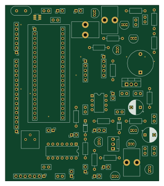
Similar boards
 AVR/Arduino
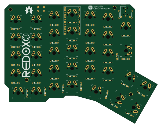
Redox keyboard
mattdibi
162.2 × 126.5 mm77 parts2LMIT2.0k AVR/Arduino
ModuleV450
stuartpittaway
30 × 61.4 mm39 parts2LCC-BY-NC-4.01.1k AVR/Arduino
V4
30 × 50 mm38 parts2LCC-BY-NC-4.01.1k AVR/Arduino
Discipline
coseyfannitutti
304.9 × 122.8 mm170 parts2LCC-BY-NC-4.01.0k AVR/Arduino
Megadesk
gcormier
41.7 × 32.2 mm23 parts2LGPL-3.0818 AVR/Arduino
Easyduino Atmega Nano
Hanqaqa
43.4 × 18 mm30 parts4LCERN-OHL-P-2.0746