
Ep2c35 trial

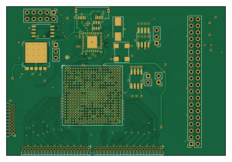
About the Ep2c35 trial PCB
Ep2c35 trial is an open source PCB design by tomverbeure, published on GitHub. It is a 4-layer board measuring 84.4 × 57.6 mm, with 180 components from 42 distinct parts.
Other key parts include the EP2C5F484, MIC37302, FT600Q-B-T, W25Q16JVSNIQ and MIC39102. By type, the board carries 73 capacitors, 71 resistors, 14 ICs, 10 connectors, 7 diodes and 3 inductors.
It belongs with the test & measurement designs in this gallery.
From the project
* Agilent - Probing Solutions for Logic Analyzers
* Agilent - Probing Solutions for Logic Analyzers
HP/Agilent 01650-61608 - Sixteen-channel probe lead set Also known as E5383A 40 pins: 16 data input, 1 clk input, 2 +5V, 1 DNC, 18 signal ground, 2 +5V ground RC network: 90k ohm/8.2pF Need board connector that is 0.425" tall 3M 8540-4500PL board connector
* Bidirectional TVS diode for protecting dual-rail power
Main components on the Ep2c35 trial
Ep2c35 trial bill of materials (BOM)
180 components, 42 distinct parts — part numbers from the project's BOM.
| Qty | Part | Footprint | Refs |
|---|---|---|---|
| 1 | EP2C5F484 EP2C35F484 | BGA-484_23.0x23.0mm_Layout22x22_P1.0mm | U1 |
| 1 | MIC37302 | S-PAK-5 | U2 |
| 1 | FT600Q-B-T | QFN-56-1EP_7x7mm_P0.4mm_FT600Q | U3 |
| 1 | W25Q16JVSNIQ | SOIC-8_5.23x5.23mm_P1.27mm | U4 |
| 1 | MIC39102 | SOICN-8LD-PL-1 | U5 |
| 1 | MIC49150-1.2 | SOICN-8LD-PL-1 | U6 |
| 1 | SP3003-02UTG | SOT-23-6 | U7 |
| 5 | SRV05-4 | SOT-23-6 | U8, U9, U10, U11, U17 |
| 2 | LM317_TO-252 | TO-252-2 | U12, U13 |
| 1 | FNETHE025 | Oscillator_SMD_IQD_IQXO70-4Pin_7.5x5.0mm | X1 |
| 1 | ABM7-30.000MHZ-D2Y-T | Crystal_SMD_0603-2Pin_6.0x3.5mm_HandSoldering | Y1 |
| 2 | CONN_02X21_ODD_EVEN Conn_02x21_Odd_Even | PinHeader_2x21_P1.27mm_Horizontal | J1, J2 |
| 1 | 3M_8540-4500PL | 3M_8540-4500PL | J3 |
| 1 | USB3_B_MICRO_AMPHENOL_GSB343K331HR USB3_B_Micro_Amphenol_GSB343K331HR | AMPHENOL_GSB343K331HR | J4 |
| 1 | CONN_02X05_ODD_EVEN Conn_02x05_Odd_Even | PinHeader_2x05_P2.54mm_Vertical | J5 |
| 1 | CONN_01X02_MALE Conn_01x03_Pin | PinHeader_1x03_P2.54mm_Vertical | J7 |
| 2 | CONN_01X02_MALE Conn_01x02_Male | PinHeader_1x02_P2.54mm_Vertical | J8, J9 |
| 1 | Conn_02x10_Odd_Even | PinHeader_2x10_P1.27mm_Horizontal | J10 |
| 1 | Conn_01x03_Pin | PinHeader_1x03_P2.54mm_Vertical | J11 |
| 7 | LED | LED_0603_1608Metric | D1, D3, D4, D5, D6, D7, D8 |
Show 22 more
| Qty | Part | Footprint | Refs |
|---|---|---|---|
| 3 | BLM18PG221SN1D | R_0603_1608Metric | FB1, FB2, FB3 |
| 5 | 1n | C_0402_1005Metric | C1, C3, C31, C33, C35 |
| 50 | 100N 100n | C_0402_1005Metric | C2, C4, C9, C10, C11, C12, C13, C14 +42 |
| 3 | 0.1U 0.1u | C_0402_1005Metric | C5, C6, C7 |
| 1 | 4.7U 4.7u | C_0402_1005Metric | C8 |
| 2 | 18P 18p | C_0402_1005Metric | C19, C20 |
| 1 | 4.7U 100n | C_0402_1005Metric | C21 |
| 2 | 2u | C_0805_2012Metric | C23, C25 |
| 2 | 47U 47u | C_1206_3216Metric | C24, C26 |
| 5 | 1u | C_0805_2012Metric | C27, C28, C29, C71, C73 |
| 1 | 10U 10u | C_0805_2012Metric | C30 |
| 1 | 100n | C_0402_1005Metric | C72 |
| 1 | 1.6k/1% | R_0402_1005Metric | R1 |
| 25 | 10K 10k | R_0402_1005Metric | R2, R3, R4, R5, R6, R7, R10, R31 +17 |
| 1 | 10K 5k | R_0402_1005Metric | R8 |
| 1 | 10K 3k | R_0402_1005Metric | R9 |
| 20 | 100 | R_0402_1005Metric | R11, R12, R13, R14, R15, R16, R17, R18 +12 |
| 7 | 1k | R_0402_1005Metric | R49, R51, R52, R53, R54, R55, R70 |
| 8 | 120 | R_0402_1005Metric | R56, R58, R59, R61, R62, R64, R65, R67 |
| 4 | 170 | R_0402_1005Metric | R57, R60, R63, R66 |
| 3 | 5k | R_0402_1005Metric | R68, R69, R71 |
| 1 | 3k | R_0402_1005Metric | R72 |
Ep2c35 trial design files
The KiCad project lives in the tomverbeure/logic_analyzer repository on GitHub; these links point at the commit this page was built from.
Ep2c35 trial: common questions
How big is the Ep2c35 trial PCB?
The Ep2c35 trial measures 84.4 × 57.6 mm, has 4 copper layers and is 1.60484 mm thick.
How many components are on the Ep2c35 trial?
180 components, from 42 distinct parts, with part numbers taken from the project's own BOM. The full bill of materials is listed on this page.
Where can I download the Ep2c35 trial design files?
From the tomverbeure/logic_analyzer repository on GitHub, which has the KiCad layout, the schematic and the BOM; the links under Design files point to each one.
Can I use the Ep2c35 trial design in my own project?
The repository has no license, so all rights stay with tomverbeure. Use it as a reference, and ask the author before reusing the design.
More boards in logic_analyzer
Similar boards
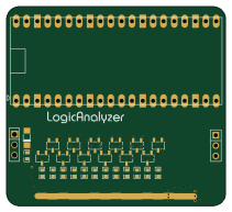
AnalyzerBoxPCB fork
gusmanb
52.7 × 47.9 mm54 parts4LGPL-3.05.0k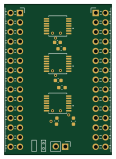
LevelShifter
28.3 × 39.8 mm21 parts2LGPL-3.05.0k
StackLink
52.3 × 10.5 mm5 parts2LGPL-3.05.0k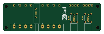
EleLab v2 Frontpanel a
Chrismettal
88 × 25 mm23 parts2LGPL-3.0528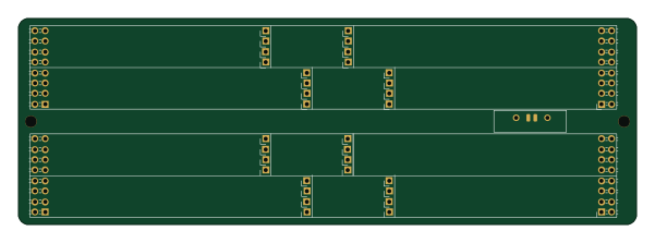
EleLab v2 Bus150
150 × 50 mm37 parts2LGPL-3.0528
EleLab v2 PowerFeed
68 × 50 mm11 parts2LGPL-3.0528