
Sbc allwinner a13

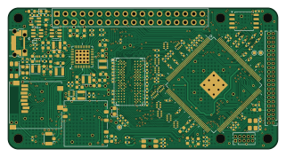
About the Sbc allwinner a13 PCB
Sbc allwinner a13 is an open source PCB design by vd-rd, published on GitHub. It is a 4-layer board measuring 80 × 42 mm, with 163 components from 42 distinct parts.
Other key parts include the USBLC6-2P6, W25Q128JVS, A13, DDR3L-x16 and RTL8188CUS. By type, the board carries 84 capacitors, 50 resistors, 10 ICs, 6 inductors, 5 connectors and 3 diodes.
It belongs with the iot & wireless, displays & leds and audio designs in this gallery.
From the project
Open hardware compute module with Allwinner A13 (ARM-A8 @1GHz), DDR3 (max 512MB) and expansions (USB, GPIO, WiFi, LCD, Audio)
A13 features a few power rails: VDD-CPU - TBD - from AXP209 VDD-INT - 1.2V - from DCDC VDD-GPIO - 3V3 - from AXP209 VDD-DRAM - 1V5 - from DCDC * AVCC - 3V - from AXP209
The datasheet states that AVCC and VDD-DRAM must be present at all times (even standby). VDD-INT and VDD-CPU can't be tied together because VDD-CPU is DVS enabled.
A13 DRAM controller doesn't provide DDR-CS. On the memory side the pin is tied to GND. Memory tuning should be performed as described here
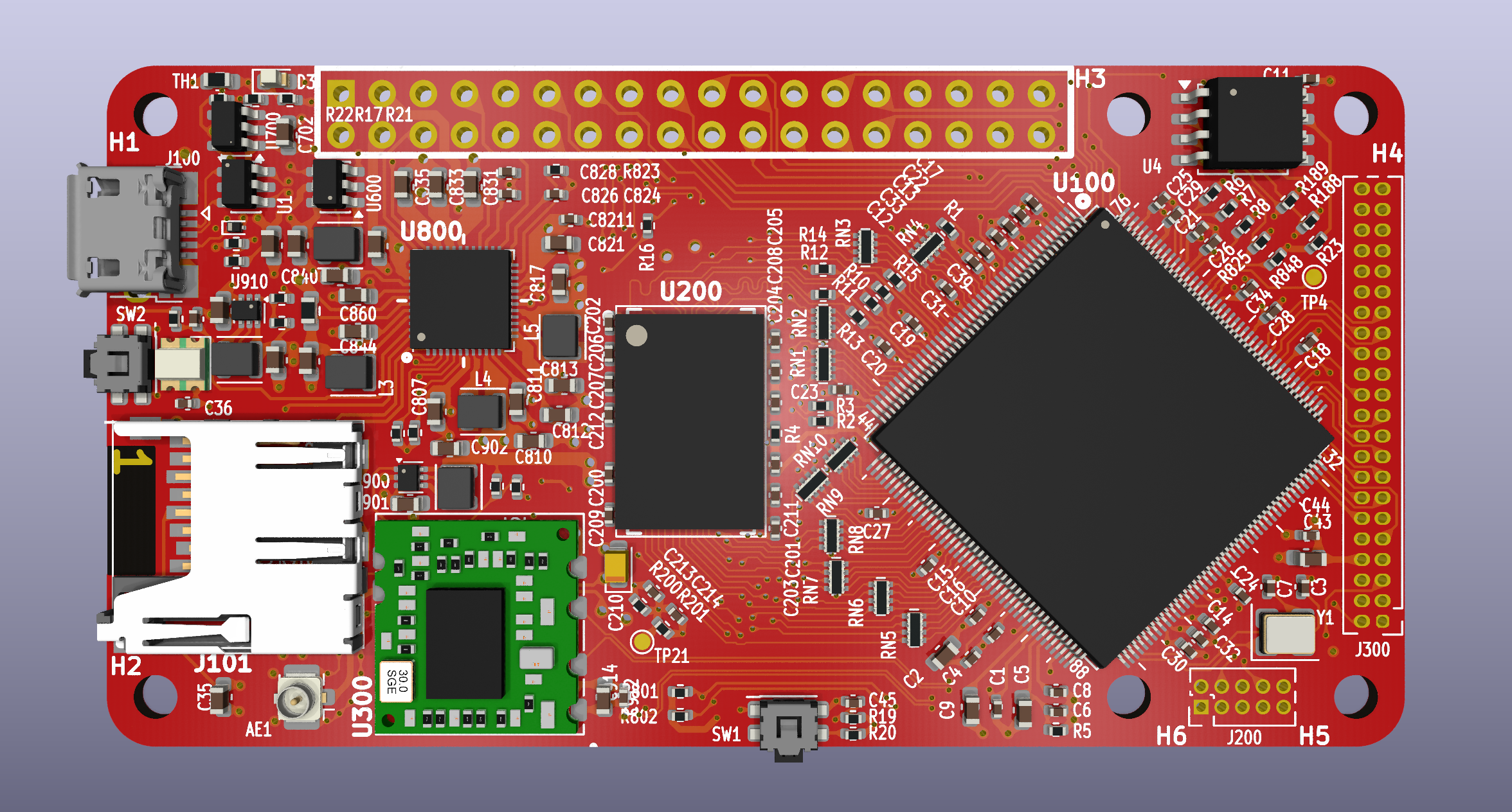
Main components on the Sbc allwinner a13
Sbc allwinner a13 bill of materials (BOM)
163 components, 42 distinct parts.
| Qty | Part | Footprint | Refs |
|---|---|---|---|
| 1 | USBLC6-2P6 | SOT-23-6 | U1 |
| 1 | W25Q128JVS | SOIC-8_5.3x5.3mm_P1.27mm | U4 |
| 1 | A13 | LQFP-176_20x20mm_P0.4mm | U100 |
| 1 | DDR3L-x16 | BGA-96_9x14mm_P0.8mm | U200 |
| 1 | RTL8188CUS | RTL8188CUS | U300 |
| 1 | MCP1640CH | SOT-23-6 | U600 |
| 1 | AP22811 | SOT-23-5 | U700 |
| 1 | AXP209 | QFN-48-1EP_6x6mm_P0.4mm_EP4.2x4.2mm_ThermalVias | U800 |
| 2 | AP61100 | SOT-563 | U900, U910 |
| 1 | 24MHz | Crystal_SMD_3225-4Pin_3.2x2.5mm | Y1 |
| 1 | Conn_02x18_Odd_Even | PinHeader_2x18_P2.54mm_Vertical | J1 |
| 1 | USB_B_Micro | USB_Micro-B_Amphenol_10103594-0001LF_Horizontal | J100 |
| 1 | Micro_SD_Card_Det | MEM20610118800A | J101 |
| 1 | Conn_02x05_Odd_Even | PinHeader_2x05_P1.27mm_Vertical | J200 |
| 1 | Conn_02x22_Odd_Even | PinHeader_2x22_P1.27mm_Vertical | J300 |
| 1 | Antenna_Shield | U.FL_Hirose_U.FL-R-SMT-1_Vertical | AE1 |
| 2 | SW_Push | SW_SPST_EVQP7C | SW1, SW2 |
| 1 | Thermistor_NTC | R_0603_1608Metric | TH1 |
| 1 | ESD9B5.0ST5G | D_SOD-923 | D2 |
| 1 | LED_Small | LED_0603_1608Metric | D3 |
Show 22 more
| Qty | Part | Footprint | Refs |
|---|---|---|---|
| 1 | LED_BAGR | LED_RGB_Optosupply_OSTB0805C1E-A-0.8T | D4 |
| 2 | 1uH | L_Wuerth_MAPI-2510 | L1, L910 |
| 1 | 4.7uH | L_Wuerth_MAPI-2510 | L2 |
| 3 | 4.7uH | L_Wuerth_MAPI-2512 | L3, L4, L5 |
| 49 | 100nF | C_0402_1005Metric | C1, C4, C6, C10, C11, C12, C13, C14 +41 |
| 21 | 10uF | C_0603_1608Metric | C2, C9, C43, C601, C701, C702, C807, C810 +13 |
| 2 | 22pF | C_0402_1005Metric | C3, C7 |
| 6 | 4.7uF | C_0603_1608Metric | C5, C811, C812, C821, C844, C860 |
| 5 | 1uF | C_0402_1005Metric | C8, C36, C824, C826, C828 |
| 1 | 100uF | CP_EIA-2012-15_AVX-P | C210 |
| 2 | 240 | R_0402_1005Metric | R1, R4 |
| 8 | 24 | R_0402_1005Metric | R2, R3, R10, R11, R12, R13, R14, R15 |
| 7 | 200k | R_0402_1005Metric | R5, R19, R22, R23, R823, R901, R911 |
| 3 | 180 | R_0402_1005Metric | R6, R7, R8 |
| 9 | 2.2k | R_0402_1005Metric | R9, R21, R188, R189, R200, R201, R801, R802 +1 |
| 5 | 47k | R_0402_1005Metric | R16, R20, R701, R825, R848 |
| 2 | 562k | R_0402_1005Metric | R17, R602 |
| 1 | 30m | R_0603_1608Metric | R18 |
| 1 | 976k | R_0402_1005Metric | R601 |
| 1 | 133k | R_0402_1005Metric | R902 |
| 1 | 44.2k | R_0402_1005Metric | R910 |
| 10 | 24 | R_Array_Concave_4x0402 | RN1, RN2, RN3, RN4, RN5, RN6, RN7, RN8 +2 |
Sbc allwinner a13 design files
The KiCad project lives in the vd-rd/sbc_allwinner_a13 repository on GitHub; these links point at the commit this page was built from.
- Layouthardware/module.kicad_pcb
- Schematichardware/module.kicad_sch
Sbc allwinner a13: common questions
How big is the Sbc allwinner a13 PCB?
The Sbc allwinner a13 measures 80 × 42 mm, has 4 copper layers and is 0.948 mm thick.
How many components are on the Sbc allwinner a13?
163 components, from 42 distinct parts. The full bill of materials is listed on this page.
Where can I download the Sbc allwinner a13 design files?
From the vd-rd/sbc_allwinner_a13 repository on GitHub, which has the KiCad layout and the schematic; the links under Design files point to each one.
Can I use the Sbc allwinner a13 design in my own project?
The repository has no license, so all rights stay with vd-rd. Use it as a reference, and ask the author before reusing the design.
Similar boards
View screen
scottbez1
35 × 35 mm12 parts2LApache-2.022.2k
BM28B0.6-24DSBreakout
15.2 × 35.6 mm3 parts2LApache-2.022.2k
LevelShifterBreakout
15.2 × 20.3 mm5 parts2LApache-2.022.2k
View base
81.2 × 81.2 mm81 parts2LApache-2.022.2k
ChainlinkDriverTester
198.1 × 95.3 mm123 parts2LApache-2.04.2k
ChainlinkBase
98.4 × 190.5 mm119 parts2LApache-2.04.2k