
SensorNode-PCB-Design

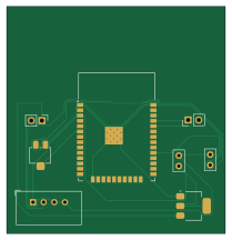
About the SensorNode-PCB-Design
SensorNode-PCB-Design is an open source ESP32 PCB design by Vinay-Kumbar, published on GitHub. It is a 2-layer board measuring 52 × 54 mm, with 8 components from 7 distinct parts.
Its main chip is the ESP32-WROOM-32, from the ESP32 family. Other key parts include the AM2302 and AMS1117-3.3. By type, the board carries 3 ICs, 2 connectors and 2 capacitors.
It belongs with the sensors and iot & wireless designs in this gallery.
From the project
PCB design for a multi-sensor node (ESP32, DHT22, vibration sensor) built in KiCad — schematic, layout, and manufacturing files
This is a PCB design for a multi-sensor node - the physical board that would hold an ESP32, a DHT22 temperature sensor, a vibration sensor input, and the power/programming circuitry needed to run them. I designed it in KiCad, going from schematic to a fully routed board with a ground plane and manufacturing-ready output files.
This is meant as a companion piece to my other project, an RTOS-based firmware system built on the same idea (ESP32 + DHT22 + vibration sensor). That project proved I can write the firmware; this one proves I can design the actual board it would run on.
Main components on the SensorNode-PCB-Design
SensorNode-PCB-Design bill of materials (BOM)
8 components, 7 distinct parts — part numbers from the project's BOM.
| Qty | Part | Footprint | Refs |
|---|---|---|---|
| 1 | ESP32-WROOM-32 | ESP32-WROOM-32 | U1 |
| 1 | AM2302 | ASAIR_AM2302_P2.54mm_Vertical | U2 |
| 1 | AMS1117-3.3 | SOT-223-3_TabPin2 | U3 |
| 1 | CONN_01X02 Conn_01x02 | PinHeader_1x02_P2.54mm_Vertical | J1 |
| 1 | CONN_01X04 Conn_01x04 | PinHeader_1x02_P2.54mm_Vertical | J2 |
| 1 | R_Potentiometer | Potentiometer_Bourns_3224X_Vertical | RV1 |
| 2 | C | C_Disc_D5.0mm_W2.5mm_P2.50mm | C1, C2 |
SensorNode-PCB-Design design files
The KiCad project lives in the Vinay-Kumbar/SensorNode-PCB-Design repository on GitHub; these links point at the commit this page was built from.
- LayoutSensorNodePCB.kicad_pcb
- SchematicSensorNodePCB.kicad_sch
- BOMSensorNodePCB_BOM.csv
SensorNode-PCB-Design: common questions
What microcontroller does the SensorNode-PCB-Design use?
The SensorNode-PCB-Design is built around the ESP32-WROOM-32, from the ESP32 family.
How big is the SensorNode-PCB-Design?
The SensorNode-PCB-Design measures 52 × 54 mm, has 2 copper layers and is 1.6 mm thick.
How many components are on the SensorNode-PCB-Design?
8 components, from 7 distinct parts, with part numbers taken from the project's own BOM. The full bill of materials is listed on this page.
Where can I download the SensorNode-PCB-Design design files?
From the Vinay-Kumbar/SensorNode-PCB-Design repository on GitHub, which has the KiCad layout, the schematic and the BOM; the links under Design files point to each one.
Can I use the SensorNode-PCB-Design design in my own project?
The repository has no license, so all rights stay with Vinay-Kumbar. Use it as a reference, and ask the author before reusing the design.
Can I test firmware for the SensorNode-PCB-Design without the hardware?
Yes. HardLabs builds a simulation of the board from its netlist and BOM, so you can run and debug ESP32 firmware against it before you order a PCB.
Similar boards
 ESP32
ESP32Open Book Abridged Edition
joeycastillo
85 × 115 mm65 parts2LCC-BY-SA-4.08.1k ESP32
ESP32Badge
atopile
56.3 × 39 mm239 parts4LMIT4.0k ESP32
ESP32Esp32 minimal
36.2 × 26.8 mm20 parts2LMIT4.0k ESP32
ESP32Racer
StuckAtPrototype
36 × 50.2 mm70 parts4LApache-2.03.8k ESP32
ESP32Controller
29 × 74 mm58 parts4LApache-2.03.8k ESP32
ESP32Bitaxe
skot
56.5 × 99.8 mm86 parts4LCERN-OHL-S-2.01.4k