
YETI60

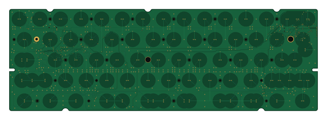
About the YETI60 PCB
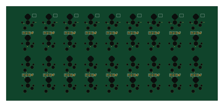
YETI60 is an open source PCB design by wZuck, published on GitHub. It is a 4-layer board measuring 285 × 94.6 mm, with 77 components from 77 distinct parts.
Other key parts include the E73-2G4M08S1C, 74HC4051, OPA350, BQ24074RGT and TPS63031DSK. By type, the board carries 43 resistors, 17 capacitors, 8 ICs, 2 connectors, 2 switches and 2 diodes.
It belongs with the power & battery and keyboards designs in this gallery.
From the project
Yet another EC Topre Input, 60% layout
One Ebyte E73-2G4M08S1C handles the intended EC scan, native USB and BLE roles. OPA350, muxes, charger and regulator are peripherals, not additional controllers. STM32 and onboard USB1 are removed; a rear Type-C daughterboard connects to J1. Original EC60 sensing geometry, outline, mounting locations and four-layer structure are retained.
Strict CAD DRC has 0 errors and 0 opens with 270 physical pin pairs connected. Local power paths use ordinary through-via routing; hardware measurements remain pending. See the comprehensive review.
Main components on the YETI60
YETI60 bill of materials (BOM)
77 components, 77 distinct parts.
| Qty | Part | Footprint | Refs |
|---|---|---|---|
| 1 | E73-2G4M08S1C | E73-2G4M08S1C__U1 | U1 |
| 1 | 74HC4051 | TSSOP16__U2 | U2 |
| 1 | OPA350 | SOIC-8_3.9x4.9mm_P1.27mm__U3 | U3 |
| 1 | 74HC4051 | TSSOP16__U4 | U4 |
| 1 | BQ24074RGT | VQFN-16-1EP_3x3mm_P0.5mm_EP1.6x1.6mm__U5 | U5 |
| 1 | TPS63031DSK | WSON-10-1EP_2.5x2.5mm_P0.5mm_EP1.2x2mm__U6 | U6 |
| 1 | TPS22919DCK | SOT-363_SC-70-6__U7 | U7 |
| 1 | TPS22919DCK | SOT-363_SC-70-6__U8 | U8 |
| 1 | REAR_USB_DAUGHTERBOARD | JST-SR-4__J1 | J1 |
| 1 | PROTECTED_1S_4V2_NTC10K | JST_PH_S3B-PH-SM4-TB_1x03-1MP_P2.00mm_Horizontal__J2 | J2 |
| 1 | 500mA | Fuse_1206_3216Metric__F1 | F1 |
| 1 | Ext_Res | R_0603_1608Metric_Pad0.98x0.95mm_HandSolder__JP1 | JP1 |
| 1 | EVQPUC02K_RESET | Panasonic_EVQPUL_EVQPUC__SW1 | SW1 |
| 1 | JS102011SAQN_POWER | SW_SPDT_CK_JS102011SAQN__SW100 | SW100 |
| 1 | PRTR5V0U2X | SOT-143__D1 | D1 |
| 1 | STATUS | LED_0603_1608Metric__D2 | D2 |
| 1 | 1.5uH_74438336015 | L_Wuerth_MAPI-3015__L1 | L1 |
| 1 | 100n | C_0402_1005Metric__C9 | C9 |
| 1 | 220p | C_0402_1005Metric__C10 | C10 |
| 1 | 100n | C_0402_1005Metric__C11 | C11 |
Show 57 more
| Qty | Part | Footprint | Refs |
|---|---|---|---|
| 1 | 100n | C_0402_1005Metric__C12 | C12 |
| 1 | 1u | C_0402_1005Metric__C13 | C13 |
| 1 | 10u/10V | C_0603_1608Metric__C30 | C30 |
| 1 | 100n/16V | C_0402_1005Metric__C31 | C31 |
| 1 | 4.7u/10V | C_0603_1608Metric__C32 | C32 |
| 1 | 1u/10V | C_0603_1608Metric__C40 | C40 |
| 1 | 10u/10V | C_0603_1608Metric__C41 | C41 |
| 1 | 10u/10V | C_0603_1608Metric__C42 | C42 |
| 1 | 10u/10V | C_0603_1608Metric__C43 | C43 |
| 1 | 100n/16V | C_0603_1608Metric__C44 | C44 |
| 1 | 10u/10V | C_0603_1608Metric__C45 | C45 |
| 1 | 10u/10V | C_0603_1608Metric__C46 | C46 |
| 1 | 10n | C_0402_1005Metric__C47 | C47 |
| 1 | 1u/10V | C_0402_1005Metric__C48 | C48 |
| 1 | 100 | R_0402_1005Metric__R3 | R3 |
| 1 | 100 | R_0402_1005Metric__R4 | R4 |
| 1 | 100 | R_0402_1005Metric__R5 | R5 |
| 1 | 100 | R_0402_1005Metric__R6 | R6 |
| 1 | 100 | R_0402_1005Metric__R7 | R7 |
| 1 | 100k | R_0402_1005Metric__R8 | R8 |
| 1 | 100k | R_0402_1005Metric__R9 | R9 |
| 1 | 100k | R_0402_1005Metric__R10 | R10 |
| 1 | 100k | R_0402_1005Metric__R11 | R11 |
| 1 | 100k | R_0402_1005Metric__R12 | R12 |
| 1 | 100k | R_0402_1005Metric__R13 | R13 |
| 1 | 100k | R_0402_1005Metric__R14 | R14 |
| 1 | 100k | R_0402_1005Metric__R15 | R15 |
| 1 | 100k | R_0402_1005Metric__R16 | R16 |
| 1 | 1k | R_0402_1005Metric__R17 | R17 |
| 1 | 100k | R_0402_1005Metric__R18 | R18 |
| 1 | 100k | R_0402_1005Metric__R19 | R19 |
| 1 | 100k | R_0402_1005Metric__R20 | R20 |
| 1 | 100k | R_0402_1005Metric__R21 | R21 |
| 1 | 100k | R_0402_1005Metric__R23 | R23 |
| 1 | 100k | R_0402_1005Metric__R24 | R24 |
| 1 | 100k | R_0402_1005Metric__R25 | R25 |
| 1 | 10k | R_0402_1005Metric__R26 | R26 |
| 1 | 0 | R_0402_1005Metric__R30 | R30 |
| 1 | 0 | R_0402_1005Metric__R31 | R31 |
| 1 | 2.2k | R_0402_1005Metric__R32 | R32 |
| 1 | 2.21k/1% | R_0402_1005Metric__R40 | R40 |
| 1 | 7.50k/1% | R_0402_1005Metric__R41 | R41 |
| 1 | 100k | R_0402_1005Metric__R42 | R42 |
| 1 | 100k | R_0402_1005Metric__R43 | R43 |
| 1 | 100k | R_0402_1005Metric__R44 | R44 |
| 1 | 100k | R_0402_1005Metric__R45 | R45 |
| 1 | 100k | R_0402_1005Metric__R46 | R46 |
| 1 | 100 | R_0402_1005Metric__R47 | R47 |
| 1 | 100k | R_0402_1005Metric__R48 | R48 |
| 1 | 100k | R_0402_1005Metric__R49 | R49 |
| 1 | 100k | R_0402_1005Metric__R50 | R50 |
| 1 | 1M/1% | R_0402_1005Metric__R51 | R51 |
| 1 | 1M/1% | R_0402_1005Metric__R52 | R52 |
| 1 | 100 | R_0402_1005Metric__R53 | R53 |
| 1 | 100 | R_0402_1005Metric__R54 | R54 |
| 1 | 69.8k/1% | R_0402_1005Metric__R55 | R55 |
| 1 | 1.69k/1% | R_0402_1005Metric__R56 | R56 |
YETI60 design files
The KiCad project lives in the wZuck/YETI60 repository on GitHub; these links point at the commit this page was built from.
YETI60: common questions
How big is the YETI60 PCB?
The YETI60 measures 285 × 94.6 mm, has 4 copper layers and is 1.6062 mm thick.
How many components are on the YETI60?
77 components, from 77 distinct parts. The full bill of materials is listed on this page.
Where can I download the YETI60 design files?
From the wZuck/YETI60 repository on GitHub, which has the KiCad layout and the schematic; the links under Design files point to each one.
Can I use the YETI60 design in my own project?
The repository has no license, so all rights stay with wZuck. Use it as a reference, and ask the author before reusing the design.
 byrantech


 google