
Amiga scandoubler v030wip

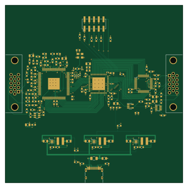
About the Amiga scandoubler v030wip PCB
Amiga scandoubler v030wip is an open source FPGA PCB design by 110-kenichi, published on GitHub. It is a 4-layer board measuring 95 × 95 mm, with 139 components from 38 distinct parts.
Its main chip is the GW1N-LV4QN88C6/I5, from the FPGA family. Other key parts include the TVP7002PZP, ADV7125KSTZ140, SN74LVC2G17DBVR, SN74LVC1G17DBVR and TPS62160DSGR. By type, the board carries 73 capacitors, 44 resistors, 9 ICs, 7 inductors, 4 connectors and 1 crystal.
It belongs with the retro computing designs in this gallery.
From the project
A1200 Line Doubler
2026-09-29 / 全配線完了・製造データ一次版 v0.30 / 製造用リリースではありません(発注前の確認が残っている)
- 変更点・検査結果・残作業:revision0.30.md(作業ログは revision0.30wip.md) - 基板:hardware/amigascandoublerv030wip.kicadpcb(KiCad 7 形式。DRC エラー0・未接続0) - 製造データ:fab/v030wip/(README に一覧と発注前の注意) - 配線レビューとシミュレーション:reviewv030wipwiring.md - ERC:hardware/erck9.rpt、除外 hardware/ercexclusions.json`
- 最新:出力側H/V同期配線:syncoutreview.md - 現行基板:hardware/amigascandoublersyncout.kicadpcb - 独立検査:hardware/syncoutreport.json、hardware/syncoutdrc.txt - 配線図:syncoutreview.png、syncoutdetail.png
Main components on the Amiga scandoubler v030wip
Amiga scandoubler v030wip bill of materials (BOM)
139 components, 38 distinct parts.
| Qty | Part | Footprint | Refs |
|---|---|---|---|
| 1 | TVP7002PZP | TQFP-100_TVP7002_14x14_P0.5_EP6.2 | U1 |
| 1 | GW1N-LV4QN88C6/I5 | QFN-88_GW1N4_10x10_P0.4_EP6.8 | U2 |
| 1 | ADV7125KSTZ140 | LQFP-48_7x7mm_P0.5mm | U3 |
| 2 | SN74LVC2G17DBVR | SOT-23-6 | U4, U5 |
| 1 | SN74LVC1G17DBVR | SOT-23-5 | U6 |
| 3 | TPS62160DSGR | WSON-8-1EP_2x2mm_P0.5mm_EP0.9x1.6mm | U7, U8, U9 |
| 1 | 27MHz OT2EL4C4JI-111OLP-27M | OSC_ECS-3225MVLC_3.2x2.5 | Y1 |
| 2 | HYC06-HDR15B-060 | DE15_HOAUC_HYC06-HDR15B-060 | J1, J2 |
| 1 | TYPE-C-31-M-12 | USB_C_Receptacle_HRO_TYPE-C-31-M-12 | J3 |
| 1 | JTAG 2x05 2.54mm | PinHeader_2x05_P2.54mm_Vertical_SMD | J4 |
| 1 | 1A hold - select | Fuse_1206_3216Metric | F1 |
| 4 | 220R@100MHz | L_0603_1608Metric | FB1, FB2, FB3, FB4 |
| 3 | 2.2uH | L_TDK_VLS4012CX | L1, L2, L3 |
| 43 | 100nF | C_0603_1608Metric | C1, C13, C14, C15, C16, C17, C18, C19 +35 |
| 1 | 4.7nF | C_0603_1608Metric | C2 |
| 3 | 1nF | C_0603_1608Metric | C3, C9, C11 |
| 7 | 10nF | C_0603_1608Metric | C4, C5, C6, C7, C8, C10, C12 |
| 6 | 4.7uF | C_0805_2012Metric | C40, C41, C62, C64, C66, C68 |
| 1 | 100nF | C_0402_1005Metric | C42 |
| 2 | 10uF | C_0805_2012Metric | C47, C54 |
Show 18 more
| Qty | Part | Footprint | Refs |
|---|---|---|---|
| 3 | 10uF 10V | C_0805_2012Metric | C55, C57, C59 |
| 3 | 22uF 10V | C_0805_2012Metric | C56, C58, C60 |
| 4 | 100nF | C_0402_1005Metric | C70, C71, C72, C73 |
| 1 | 1.5k | R_0603_1608Metric | R1 |
| 9 | 4.7k | R_0603_1608Metric | R2, R3, R4, R5, R6, R7, R8, R9 +1 |
| 1 | 536R 0.1% | R_0603_1608Metric | R10 |
| 6 | 75R 0.1% | R_0603_1608Metric | R11, R12, R13, R15, R16, R17 |
| 6 | 10k | R_0603_1608Metric | R14, R33, R34, R41, R42, R43 |
| 4 | 33R | R_0603_1608Metric | R18, R20, R22, R23 |
| 3 | 100k | R_0603_1608Metric | R19, R21, R35 |
| 2 | 22R | R_0603_1608Metric | R24, R36 |
| 2 | 5.1k 1% | R_0603_1608Metric | R25, R26 |
| 1 | 312k 0.1% | R_0603_1608Metric | R27 |
| 3 | 100k 0.1% | R_0603_1608Metric | R28, R30, R32 |
| 1 | 137k 0.1% | R_0603_1608Metric | R29 |
| 1 | 49.9k 0.1% | R_0603_1608Metric | R31 |
| 2 | 2.2k | R_0402_1005Metric | R37, R38 |
| 2 | 10k | R_0402_1005Metric | R39, R40 |
Amiga scandoubler v030wip design files
The KiCad project lives in the 110-kenichi/A1200LineDoubler repository on GitHub; these links point at the commit this page was built from.
Amiga scandoubler v030wip: common questions
What microcontroller does the Amiga scandoubler v030wip use?
The Amiga scandoubler v030wip is built around the GW1N-LV4QN88C6/I5, from the FPGA family.
How big is the Amiga scandoubler v030wip PCB?
The Amiga scandoubler v030wip measures 95 × 95 mm, has 4 copper layers and is 1.6 mm thick.
How many components are on the Amiga scandoubler v030wip?
139 components, from 38 distinct parts. The full bill of materials is listed on this page.
Where can I download the Amiga scandoubler v030wip design files?
From the 110-kenichi/A1200LineDoubler repository on GitHub, which has the KiCad layout; the links under Design files point to each one.
Can I use the Amiga scandoubler v030wip design in my own project?
The repository has no license, so all rights stay with 110-kenichi. Use it as a reference, and ask the author before reusing the design.
Can I test firmware for the Amiga scandoubler v030wip without the hardware?
Yes. HardLabs builds a simulation of the board from its netlist and BOM, so you can run and debug FPGA firmware against it before you order a PCB.
More boards in A1200LineDoubler
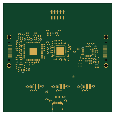 FPGA
Amiga scandoubler analog
95 × 95 mm135 parts4LNo license0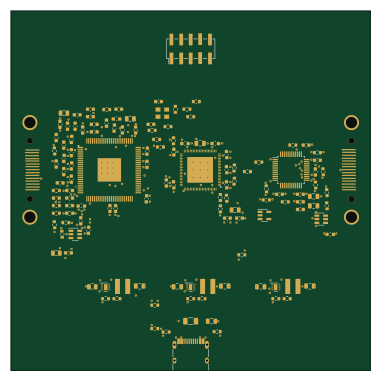 FPGA
Amiga scandoubler u2rot
95 × 95 mm135 parts4LNo license0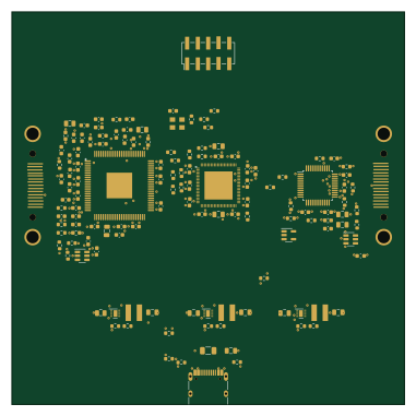 FPGA
Amiga scandoubler sync in
95 × 95 mm135 parts4LNo license0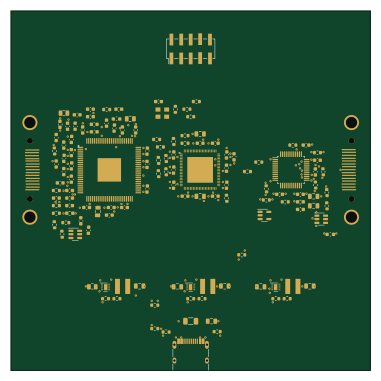 FPGA
Amiga scandoubler sync out
95 × 95 mm135 parts4LNo license0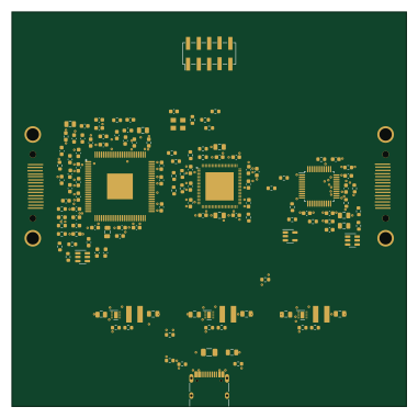 FPGA
Amiga scandoubler rgb out
95 × 95 mm135 parts4LNo license0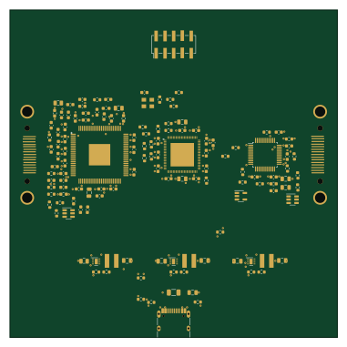 FPGA
Amiga scandoubler pll top
95 × 95 mm135 parts4LNo license0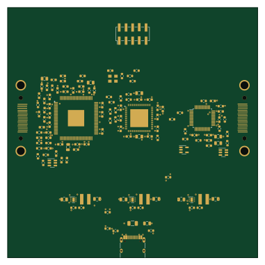 FPGA
Amiga scandoubler refined
95 × 95 mm135 parts4LNo license0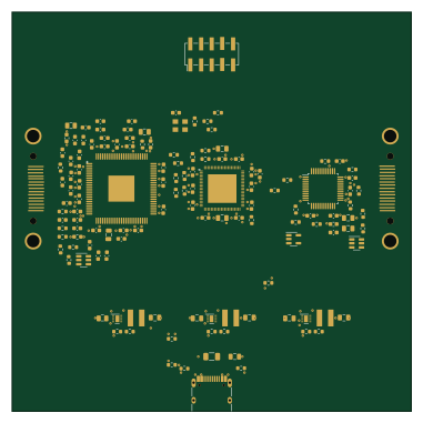 FPGA
Amiga scandoubler distribution
95 × 95 mm135 parts4LNo license0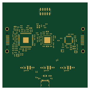 FPGA
Amiga scandoubler routing
95 × 95 mm135 parts4LNo license0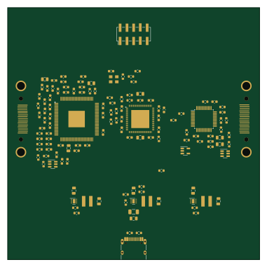 FPGA
Amiga scandoubler placement
95 × 95 mm135 parts4LNo license0
Similar boards
 FPGA
Base board
GlasgowEmbedded
80 × 49 mm222 parts4L0BSD2.2k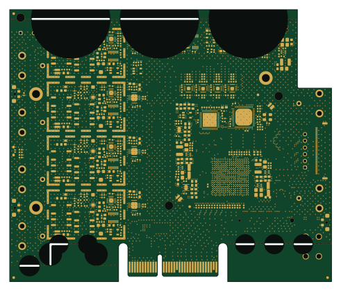 FPGA
Thunderscope Rev5.3
EEVengers
122.5 × 103.5 mm817 parts6LMIT1.3k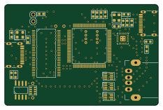 FPGA
Usb sniffer
ataradov
58.2 × 38.1 mm86 parts2LBSD-3-Clause1.3k FPGA
Tomu, I'm
theacodes
13 × 9.4 mm40 parts4LMIT1.1k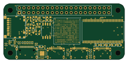 FPGA
Icepi zero
cheyao
65 × 30 mm143 parts4LSHL-2.1828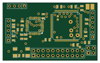 FPGA
Gcvideo
ikorb
49 × 30 mm44 parts4LNo license765