
RP2040-Dev-Board

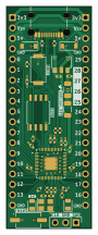
About the RP2040-Dev-Board
RP2040-Dev-Board is an open source RP2040/RP2350 PCB design by abhinav937, published on GitHub under the MIT license. It is a 4-layer board measuring 20.6 × 54 mm, with 41 components from 18 distinct parts.
Its main chip is the RP2040, from the RP2040/RP2350 family. Other key parts include the AP1117-33 and W25Q32JVSS. By type, the board carries 17 capacitors, 10 resistors, 4 connectors, 4 diodes, 3 ICs and 2 switches.
It belongs with the dev boards & breakouts designs in this gallery.
From the project
PCB Design of Breadboard friendly RP2040 Dev Board with USB-C.
Layer 1: Front Cu Layer 2: Gnd Layer 3: Gnd Layer 4: Back Cu
Initially my designs had inner layers as gnd and 3.3V, I got some netlist parity when I uploaded to my PCB manufacturer. But KiCad wasn't showing any errors in DRC, So I made both layers as Gnd. #### Manufacturing All components were purchased in lcsc.com except RP2040, Which I purchased locally for 80Rs(~$1)/μC from robu.in.

Main components on the RP2040-Dev-Board
RP2040-Dev-Board bill of materials (BOM)
41 components, 18 distinct parts — part numbers from the project's BOM.
| Qty | Part | Footprint | Refs |
|---|---|---|---|
| 1 | RP2040 | QFN40P700X700X90-57N | U1 |
| 1 | AP1117-33 | SOT-89-3 | U2 |
| 1 | W25Q32JVSS | SOIC-8_5.23x5.23mm_P1.27mm | U3 |
| 1 | 12MHz | Crystal_SMD_3225-4Pin_3.2x2.5mm | Y1 |
| 1 | USB_C_Receptacle_USB2.0 | USB_C_Receptacle_Palconn_UTC16-G | J1 |
| 2 | Conn_01x19_Male | PinHeader_1x19_P2.54mm_Vertical | J2, J4 |
| 1 | Conn_01x03_Male | PinHeader_1x03_P2.54mm_Vertical | J3 |
| 2 | PTS 636 | PTS636SK25FSMTRLFS | SW1, SW2 |
| 1 | Red | LED_0805_2012Metric | D3 |
| 2 | B5819W SL | D_SOD-123 | D4, D5 |
| 1 | Green | LED_0805_2012Metric | D6 |
| 13 | 10uF | C_0402_1005Metric | C1, C2, C5, C7, C8, C9, C10, C11 +5 |
| 2 | 27pF | C_0402_1005Metric | C3, C4 |
| 2 | 100uF | C_1206_3216Metric | C6, C12 |
| 3 | 1k | R_0402_1005Metric | R1, R6, R10 |
| 2 | 5.1k | R_0402_1005Metric | R2, R3 |
| 2 | 27 | R_0402_1005Metric | R4, R5 |
| 3 | 10k | R_0402_1005Metric | R7, R8, R9 |
RP2040-Dev-Board design files
The KiCad project lives in the abhinav937/RP2040-Dev-Board repository on GitHub; these links point at the commit this page was built from.
RP2040-Dev-Board: common questions
What microcontroller does the RP2040-Dev-Board use?
The RP2040-Dev-Board is built around the RP2040, from the RP2040/RP2350 family.
How big is the RP2040-Dev-Board?
The RP2040-Dev-Board measures 20.6 × 54 mm, has 4 copper layers and is 1.532 mm thick.
How many components are on the RP2040-Dev-Board?
41 components, from 18 distinct parts, with part numbers taken from the project's own BOM. The full bill of materials is listed on this page.
Where can I download the RP2040-Dev-Board design files?
From the abhinav937/RP2040-Dev-Board repository on GitHub, which has the KiCad layout, the schematic and the BOM; the links under Design files point to each one.
Can I use the RP2040-Dev-Board design in my own project?
Yes, under the terms of its MIT license, which abhinav937 chose for the repository.
Can I test firmware for the RP2040-Dev-Board without the hardware?
Yes. HardLabs builds a simulation of the board from its netlist and BOM, so you can run and debug RP2040/RP2350 firmware against it before you order a PCB.
Similar boards
 RP2040/RP2350
Open Book Abridged Edition
joeycastillo
85 × 115 mm29 parts2LCC-BY-SA-4.08.1k RP2040/RP2350
Corne
foostan
277.2 × 107.5 mm164 parts2LCC-BY-4.07.7k RP2040/RP2350
Corne
277.2 × 107.5 mm164 parts2LCC-BY-4.07.7k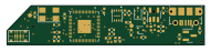 RP2040/RP2350
Msa
Mentra-Community
47.8 × 9.4 mm53 parts2LMIT1.2k RP2040/RP2350
Open Source Smart Glasses
93 × 10.5 mm80 parts4LMIT1.2k RP2040/RP2350
MSA
30.5 × 138 mm61 parts2LMIT1.2k