
Abn6502

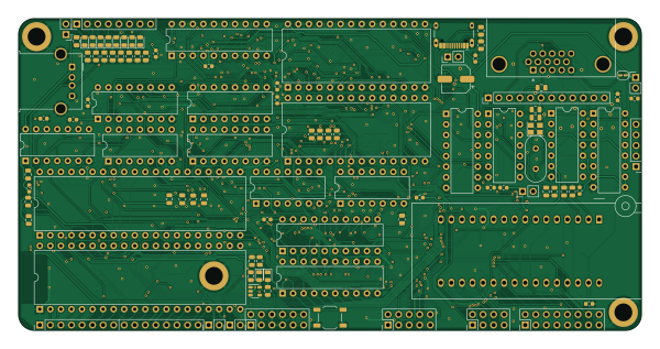
About the Abn6502 PCB
Abn6502 is an open source PCB design by AndersBNielsen, published on GitHub under the CC-BY-NC-4.0 license. It is a 2-layer board measuring 149.9 × 74.9 mm, with 142 components from 55 distinct parts.
Other key parts include the 74HC14, R6502, 74HC245, SST39SF010 and 74HC109. By type, the board carries 55 resistors, 37 capacitors, 21 ICs, 16 connectors, 10 LEDs and 2 crystals.
It belongs with the retro computing designs in this gallery.
From the project
Solving the global IC shortage by reusing old stuff!
This is a 6502-based complete single board computer intended to help during the global IC shortage. Why use new chips when you can reuse scrap?
All gold plated (ENIG) PCBs: https://www.imania.dk/index.php?currency=EUR&cPath=204&sort=5a&language=en
Check out the NEW project on HackADay if you want to read more and see some pretty pictures :)
https://hackaday.io/project/184725-abn6502-sbc-r1

Main components on the Abn6502
Abn6502 bill of materials (BOM)
142 components, 55 distinct parts — part numbers from the project's BOM.
| Qty | Part | Footprint | Refs |
|---|---|---|---|
| 1 | 74HC14 | DIP-14_W7.62mm | U1 |
| 1 | R6502 | DIP-40_W15.24mm | U2 |
| 1 | R6502 R6522 | DIP-40_W15.24mm | U3 |
| 1 | 74HC245 74HC273 | DIP-20_W7.62mm | U4 |
| 1 | SST39SF010 | DIP_Socket-32_W11.9_W12.7_W15.24_W17.78_W18.5_3M_232-1285-00-0602J | U5 |
| 2 | 74HC109 74HC590 | DIP-16_W7.62mm | U6, U7 |
| 1 | 74HC14 74HC32 | DIP-14_W7.62mm | U8 |
| 1 | NRF24L01_BREAKOUT NRF24L01_Breakout | NRF24L01-SMD | U9 |
| 2 | 74HC245 | DIP-20_W7.62mm | U10, U11 |
| 1 | 74HC109 | DIP-16_W7.62mm | U12 |
| 1 | 74HC14 74HC74 | DIP-14_W7.62mm | U13 |
| 1 | 74HC14 74HC04 | DIP-14_W7.62mm | U14 |
| 1 | MIC5504-3.3YM5 | SOT-23-5 | U15 |
| 1 | 62256 | DIP-28_W15.24mm | U16 |
| 2 | 74HC14 74HC00 | DIP-14_W7.62mm | U17, U21 |
| 1 | 62256 w27C512 | DIP-28_W15.24mm | U18 |
| 1 | 74HC109 74LS161 | DIP-16_W7.62mm | U19 |
| 1 | 74HC109 74HC165 | DIP-16_W7.62mm | U20 |
| 1 | 16Mhz | Crystal_HC49-U_Vertical | Y1 |
| 1 | 16MHZ 16Mhz | Crystal_SMD_3225-4Pin_3.2x2.5mm | Y2 |
Show 35 more
| Qty | Part | Footprint | Refs |
|---|---|---|---|
| 2 | 5V | PinHeader_1x02_P2.54mm_Vertical | J1, J8 |
| 1 | C7500783 PORTAB | PinHeader_1x16_P2.54mm_Vertical | J2 |
| 1 | C7499322 CA | PinHeader_1x02_P2.54mm_Vertical | J3 |
| 1 | C7499322 CB | PinHeader_1x02_P2.54mm_Vertical | J4 |
| 1 | W27c512? | PinHeader_1x02_P2.54mm_Vertical | J5 |
| 1 | Conn_01x12_Male | PinHeader_1x12_P2.54mm_Vertical | J7 |
| 1 | USB2.0_16P | USB_C_Receptacle_HCTL_HC-TYPE-C-16P-01A | J9 |
| 1 | USB | PinHeader_1x02_P2.54mm_Vertical | J10 |
| 1 | GPCO | PinHeader_1x05_P2.54mm_Vertical | J11 |
| 1 | Control_bus | PinHeader_1x08_P2.54mm_Vertical | J12 |
| 1 | C92269 Power | PinHeader_2x06_P2.54mm_Vertical | J14 |
| 1 | C92271 Data_bus | PinHeader_2x04_P2.54mm_Vertical | J15 |
| 1 | C30734 Address bus | PinHeader_2x08_P2.54mm_Vertical | J16 |
| 1 | C456018 USB_A | USB_A_Molex_67643_Horizontal | J17 |
| 1 | C2685204 Interface | PinHeader_2x05_P2.54mm_Vertical | J20 |
| 1 | SW_Push | SW_SPST_TL3342 | SW1 |
| 1 | 3v3 | LED_0805_2012Metric | 3v3 |
| 1 | 5v | LED_0805_2012Metric | 5V0 |
| 8 | 3V3 RED | LED_0805_2012Metric | DCTRL3, DCTRL4, DCTRL5, DCTRL6, DCTRL7, DVB0, DVB1, DVEN1 |
| 2 | 14PF 14pF | C_0805_2012Metric | C1, C2 |
| 17 | 100NF 100nF | C_0603_1608Metric | C3, C4, C5, C6, C7, C8, C9, C10 +9 |
| 1 | 220UF 220uF | CP_Elec_6.3x7.7 | C12 |
| 4 | 1UF 1uF | C_0805_2012Metric | C13, C14, C20, C21 |
| 1 | 10UF 10uF | C_0805_2012Metric | C22 |
| 12 | NC | C_0805_2012Metric | C26, C27, C28, C29, C30, C31, C32, C33 +4 |
| 16 | 3k | R_0805_2012Metric | R1, R2, R3, R4, R8, R9, R10, R11 +8 |
| 1 | 1M | R_0805_2012Metric | R5 |
| 1 | 470 | R_0805_2012Metric | R6 |
| 1 | 150 | R_0805_2012Metric | R7 |
| 1 | 150K 150k | R_0805_2012Metric | R12 |
| 3 | 2k2 | R_0805_2012Metric | R13, R15, R18 |
| 6 | 2K2 2k2 | R_0805_2012Metric | R14, R17, R22, R23, R24, R25 |
| 5 | NC | R_0805_2012Metric | R16, R19, R20, R21, R49 |
| 19 | NC | SolderJumper-2_P1.3mm_Open_RoundedPad1.0x1.5mm | R29, R30, R31, R32, R33, R34, R35, R36 +11 |
| 2 | 5K1 5k1 | R_0805_2012Metric | R58, R59 |
Abn6502 design files
The KiCad project lives in the AndersBNielsen/abn6502 repository on GitHub; these links point at the commit this page was built from.
Abn6502: common questions
How big is the Abn6502 PCB?
The Abn6502 measures 149.9 × 74.9 mm, has 2 copper layers and is 1.6 mm thick.
How many components are on the Abn6502?
142 components, from 55 distinct parts, with part numbers taken from the project's own BOM. The full bill of materials is listed on this page.
Where can I download the Abn6502 design files?
From the AndersBNielsen/abn6502 repository on GitHub, which has the KiCad layout, the schematic and the BOM; the links under Design files point to each one.
Can I use the Abn6502 design in my own project?
It is published under CC-BY-NC-4.0, which limits how it may be reused; read the license before building on it.
Similar boards
OpenTendo
Redherring32
196.3 × 118.7 mm93 parts2LTAPR-OHL-1.0850
24pin flex interposer
Wren6991
29 × 32 mm3 parts2LNo license508
Sram dev board
50 × 50 mm12 parts2LNo license508
GB-BRK-SLOT-A
Gekkio
81 × 80 mm20 parts2LCC-BY-4.0376
GB-BRK-SLOT-B
81 × 80 mm20 parts2LCC-BY-4.0376
GB-BRK-CPU-G2
80 × 80 mm12 parts2LCC-BY-4.0376