
Phono adc eval

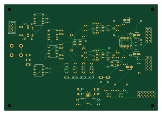
About the Phono adc eval PCB
Phono adc eval is an open source PCB design by birdybro, published on GitHub under the GPL-3.0 license. It is a 4-layer board measuring 130 × 90 mm, with 119 components from 49 distinct parts.
Other key parts include the TPS7A39DSCR, TPS7A2050PDBVR, TPS7A2033PDBVR, OPA1656IDR and OPA1632DR. By type, the board carries 48 capacitors, 44 resistors, 8 ICs, 6 diodes, 5 connectors and 4 transistors.
It belongs with the audio designs in this gallery.
From the project
FPGA based audiophile phono preamp and amp integrated unit idea. WIP
This directory contains a routed four-layer KiCad 10 evaluation board for the flat-gain Architecture A input path. It is a concrete bench prototype, not a production fabrication release and not evidence of measured performance.
The board is 130 x 90 mm with F.Cu / continuous L2 GND / L3 POWER_SIG / B.Cu. Cartridge entry, relay loading, flat gain, differential drivers, ADC, local post-regulation, and digital headers are physically partitioned. The RCA and turntable-ground connectors are EVT harness/terminal choices; production parts remain enclosure decisions.
Main components on the Phono adc eval
Phono adc eval bill of materials (BOM)
119 components, 49 distinct parts — part numbers from the project's BOM.
| Qty | Part | Footprint | Refs |
|---|---|---|---|
| 1 | TPS7A39DSCR | Texas_DSC0010J_ThermalVias | U1 |
| 1 | TPS7A2050PDBVR | SOT-23-5 | U2 |
| 1 | TPS7A2033PDBVR | SOT-23-5 | U3 |
| 2 | OPA1656IDR | SOIC-8_3.9x4.9mm_P1.27mm | U4, U8 |
| 2 | OPA1632DR | SOIC-8_3.9x4.9mm_P1.27mm | U5, U6 |
| 1 | PCM4202DBR | SSOP-28_5.3x10.2mm_P0.65mm | U7 |
| 4 | MMBT3904 | SOT-23 | Q1, Q2, Q3, Q4 |
| 1 | ISOLATED_PANEL_RCA_HARNESS | JST_XH_B3B-XH-A_1x03_P2.50mm_Vertical | J1 |
| 1 | TURNTABLE_GROUND_POST | TerminalBlock_MetzConnect_360425_1x01_Horizontal_ScrewM4.0_Boxed | J2 |
| 1 | ADC_AUDIO | PinHeader_2x05_P2.54mm_Vertical | J3 |
| 1 | POWER_INPUT | PinHeader_2x06_P2.54mm_Vertical | J4 |
| 1 | ADC_CONTROL | PinHeader_2x05_P2.54mm_Vertical | J5 |
| 1 | G6K-2F-Y-5V_GAIN_BANK | Relay_DPDT_Omron_G6K-2F-Y | K1 |
| 1 | G6K-2F-Y-5V_GAIN_RANGE | Relay_DPDT_Omron_G6K-2F-Y | K2 |
| 1 | G6K-2F-Y-5V_CAP47 | Relay_DPDT_Omron_G6K-2F-Y | K3 |
| 1 | G6K-2F-Y-5V_CAP100 | Relay_DPDT_Omron_G6K-2F-Y | K4 |
| 2 | PESD5V0X1BCL_EVT | D_SOD-882 | D1, D2 |
| 4 | 1N4148W | D_SOD-123 | D3, D4, D5, D6 |
| 2 | 47pF_C0G_1% | C_0603_1608Metric | C1, C2 |
| 2 | 100pF_C0G_1% | C_0603_1608Metric | C3, C4 |
Show 29 more
| Qty | Part | Footprint | Refs |
|---|---|---|---|
| 2 | DNP_22PF_C0G_RF DNP_22pF_C0G_RF | C_0603_1608Metric | C5, C6 |
| 4 | 1NF_C0G 1nF_C0G | C_0603_1608Metric | C20, C21, C30, C31 |
| 2 | 2.7NF_C0G 2.7nF_C0G | C_0603_1608Metric | C22, C32 |
| 4 | 100PF_C0G 100pF_C0G | C_0603_1608Metric | C23, C24, C33, C34 |
| 4 | 33UF_LOW_ESR 33uF_LOW_ESR | C_Elec_4x5.8 | C40, C42, C46, C48 |
| 10 | 100NF_X7R 100nF_X7R | C_0603_1608Metric | C41, C43, C44, C45, C47, C49, C71, C72 +2 |
| 3 | 10NF_X7R 10nF_X7R | C_0603_1608Metric | C60, C61, C62 |
| 6 | 10UF_25V_X7R 10uF_25V_X7R | C_1206_3216Metric | C63, C64, C65, C66, C79, C80 |
| 4 | 1UF_X7R 1uF_X7R | C_0603_1608Metric | C67, C68, C69, C70 |
| 4 | 100NF_X7R 100nF_X7R | C_0402_1005Metric | C73, C74, C75, C76 |
| 1 | DNP_100NF_CHASSIS DNP_100nF_CHASSIS | C_1206_3216Metric | C81 |
| 2 | 100R_0.1% | R_0805_2012Metric | R1, R2 |
| 2 | 47.5k_0.1%_25ppm | R_0805_2012Metric | R3, R4 |
| 2 | 19.1k_0.1% | R_0805_2012Metric | R5, R6 |
| 2 | 1.00k_0.1% | R_0805_2012Metric | R7, R8 |
| 2 | 2.12k_0.1% | R_0805_2012Metric | R9, R10 |
| 2 | 492R_0.1% | R_0805_2012Metric | R11, R12 |
| 8 | 316R_0.1% | R_0603_1608Metric | R20, R21, R22, R23, R30, R31, R32, R33 |
| 4 | 40.2R_0.1% | R_0603_1608Metric | R24, R25, R34, R35 |
| 1 | 22R | R_0402_1005Metric | R40 |
| 3 | 33R | R_0402_1005Metric | R41, R42, R43 |
| 5 | 100K 100k | R_0603_1608Metric | R44, R55, R56, R57, R58 |
| 1 | 10K 10k | R_0603_1608Metric | R45 |
| 4 | 2.2K 2.2k | R_0603_1608Metric | R51, R52, R53, R54 |
| 1 | 90.9k_0.1% | R_0603_1608Metric | R60 |
| 2 | 10.0k_0.1% | R_0603_1608Metric | R61, R63 |
| 1 | 100k_0.1% | R_0603_1608Metric | R62 |
| 1 | 0R_CHASSIS_BOND | R_1206_3216Metric | R70 |
| 1 | DNP_10R_CHASSIS | R_1206_3216Metric | R71 |
Phono adc eval design files
The KiCad project lives in the birdybro/FPGA_Amp repository on GitHub; these links point at the commit this page was built from.
Phono adc eval: common questions
How big is the Phono adc eval PCB?
The Phono adc eval measures 130 × 90 mm, has 4 copper layers and is 1.6 mm thick.
How many components are on the Phono adc eval?
119 components, from 49 distinct parts, with part numbers taken from the project's own BOM. The full bill of materials is listed on this page.
Where can I download the Phono adc eval design files?
From the birdybro/FPGA_Amp repository on GitHub, which has the KiCad layout, the schematic and the BOM; the links under Design files point to each one.
Can I use the Phono adc eval design in my own project?
Yes, under the terms of its GPL-3.0 license, which birdybro chose for the repository.
More boards in FPGA_Amp
Similar boards
OtterCastAudioV2
Ottercast
50 × 49.3 mm216 parts4LMIT665
FunBox
GuitarML
59.7 × 67.5 mm63 parts2LMIT278
Eurorack pmod
apfaudio
35 × 110 mm116 parts4LCERN-OHL-S-2.0239
XassetteAsterisk
SdtElectronics
56 × 56 mm137 parts2LCERN-OHL-W-2.0229
AddOnC
freeDSP
380 × 45 mm97 parts2LCC-BY-SA-4.0222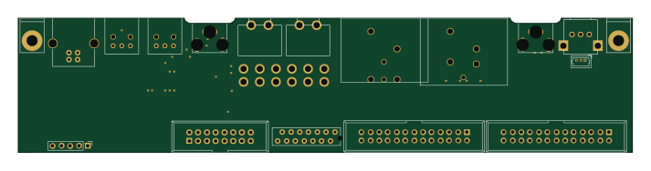
AddOnA
178 × 39 mm55 parts2LCC-BY-SA-4.0222