
RP2040-designguide

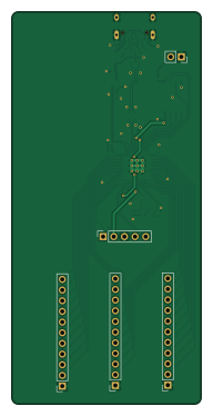
About the RP2040-designguide PCB
RP2040-designguide is an open source RP2040/RP2350 PCB design by calliah333, published on GitHub under the MIT license. It is a 2-layer board measuring 45.2 × 93.4 mm, with 31 components from 14 distinct parts.
Its main chip is the RP2040, from the RP2040/RP2350 family. Other key parts include the W25Q128JVS, USBLC6-2SC6 and XC6206PxxxMR-Regulator_Linear. By type, the board carries 17 capacitors, 7 resistors, 4 ICs, 1 crystal, 1 connector and 1 fuse.
It belongs with the keyboards designs in this gallery.
From the project
Hardware design for the RP2040
This guide requires you to have prerequisite knowledge about PCB design and a little about the RP2040. This is not a guide for absolute beginners and should not be treated as one.
I have multiple tested and working boards using the RP2040, including an open source one you can find here!
Bit of a disclaimer: I have mostly switched from RP2040 over to STM32F072 due to a few reasons. Mostly component cost and the amount of parts necessary, as well as overall stability. I have a tested and OSH f072 PCBs available on github. Namely here, here, and here. Designing with f072 is generally easier as…
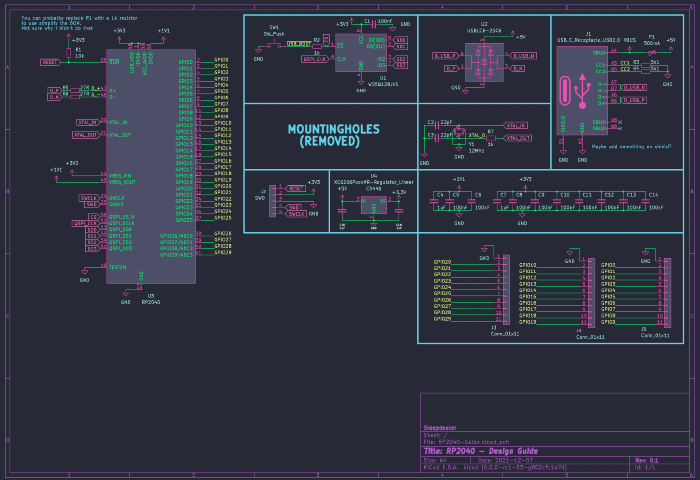
Main components on the RP2040-designguide
RP2040-designguide bill of materials (BOM)
31 components, 14 distinct parts.
| Qty | Part | Footprint | Refs |
|---|---|---|---|
| 1 | W25Q128JVS | SOIC-8_5.23x5.23mm_P1.27mm | U1 |
| 1 | USBLC6-2SC6 | SOT-23-6 | U2 |
| 1 | RP2040 | RP2040-QFN-56 | U3 |
| 1 | XC6206PxxxMR-Regulator_Linear | SOT-23 | U4 |
| 1 | 12MHz | Crystal_SMD_3225-4Pin_3.2x2.5mm | Y1 |
| 1 | USB_C_Receptacle_USB2.0 | USB_C_Receptacle_HRO_TYPE-C-31-M-12 | J1 |
| 1 | 500mA | Fuse_1206_3216Metric | F1 |
| 10 | 100nF | C_0402_1005Metric | C1, C5, C6, C9, C10, C11, C12, C13 +2 |
| 2 | 22pF | C_0402_1005Metric | C2, C3 |
| 4 | 1uF | C_0402_1005Metric | C4, C8, C16, C17 |
| 1 | 10uF | C_0402_1005Metric | C7 |
| 3 | 1k | R_0402_1005Metric | R1, R2, R7 |
| 2 | 5k1 | R_0402_1005Metric | R3, R4 |
| 2 | 27R | R_0603_1608Metric | R5, R6 |
RP2040-designguide design files
The KiCad project lives in the calliah333/RP2040-designguide repository on GitHub; these links point at the commit this page was built from.
- LayoutPCB/RP2040-Guide.kicad_pcb
- SchematicPCB/RP2040-Guide.kicad_sch
RP2040-designguide: common questions
What microcontroller does the RP2040-designguide use?
The RP2040-designguide is built around the RP2040, from the RP2040/RP2350 family.
How big is the RP2040-designguide PCB?
The RP2040-designguide measures 45.2 × 93.4 mm, has 2 copper layers and is 1.6 mm thick.
How many components are on the RP2040-designguide?
31 components, from 14 distinct parts. The full bill of materials is listed on this page.
Where can I download the RP2040-designguide design files?
From the calliah333/RP2040-designguide repository on GitHub, which has the KiCad layout and the schematic; the links under Design files point to each one.
Can I use the RP2040-designguide design in my own project?
Yes, under the terms of its MIT license, which calliah333 chose for the repository.
Can I test firmware for the RP2040-designguide without the hardware?
Yes. HardLabs builds a simulation of the board from its netlist and BOM, so you can run and debug RP2040/RP2350 firmware against it before you order a PCB.
Similar boards
 RP2040/RP2350
Open Book Abridged Edition
joeycastillo
85 × 115 mm29 parts2LCC-BY-SA-4.08.1k RP2040/RP2350
Corne
foostan
277.2 × 107.5 mm164 parts2LCC-BY-4.07.7k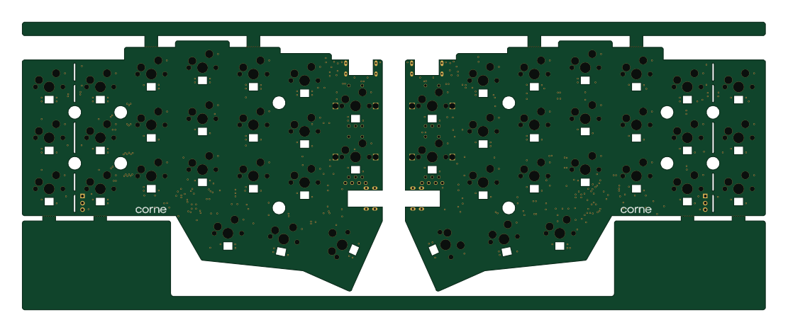 RP2040/RP2350
Corne
277.2 × 107.5 mm164 parts2LCC-BY-4.07.7k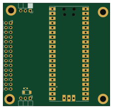 RP2040/RP2350
LogicAnalyzer
gusmanb
57 × 55.2 mm6 parts2LGPL-3.05.0k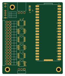 RP2040/RP2350
Jitx design
55.5 × 65 mm26 parts4LGPL-3.05.0k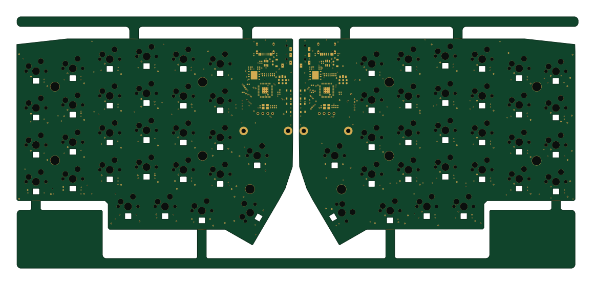 RP2040/RP2350
Pro V2
kata0510
290.1 × 130 mm270 parts2LMIT2.3k