
Trs80 fpga card

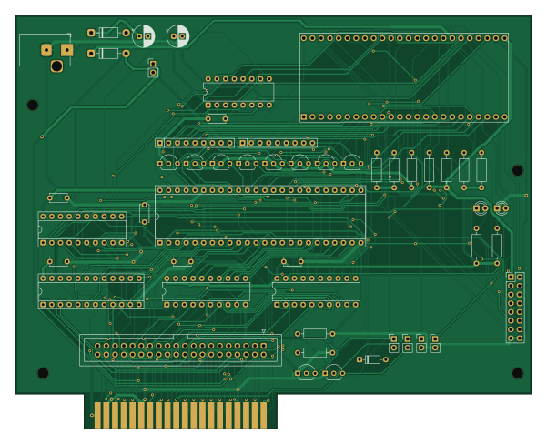
About the Trs80 fpga card PCB
Trs80 fpga card is an open source PCB design by davidellwood, published on GitHub under the MIT license. It is a 2-layer board measuring 150 × 120 mm, with 52 components from 29 distinct parts.
Other key parts include the IDT7132SA/LA (2Kx8 DPRAM), 74HCT245 RAM<->BUS, 74HCT245 PORT<->BUS, ATF22V10C-15PU MEM_DECODE and ATF16V8B-15PU IO_DECODE. By type, the board carries 13 resistors, 10 transistors, 8 capacitors, 7 ICs, 5 jumpers and 5 diodes.
It belongs with the retro computing designs in this gallery.
From the project
TRS-80 Model I expansion system: ECB backplane, Tang Nano 20K sprite/Am9511 card, FreHD-compatible SD card, 512K banked memory - all through-hole
All-through-hole hardware, FPGA design, firmware and Z80 software for the TRS-80 Model I.
- Rev 2 (current): three ECB Eurocard daughter cards, with two ways to connect them to the Model I. The design is in docs/rev2-architecture.md. - The custom backplane: 5 slots, 4 layers, with an Expansion Interface pass-through. - The bridge card: plugs into a standard ECB backplane. The Model I connects by ribbon to a right-angle header, and there's no EI. - Rev 0.1: the original single card on a Tang Nano 9K. It remains here as a working reference; see docs/hardware-design.md.
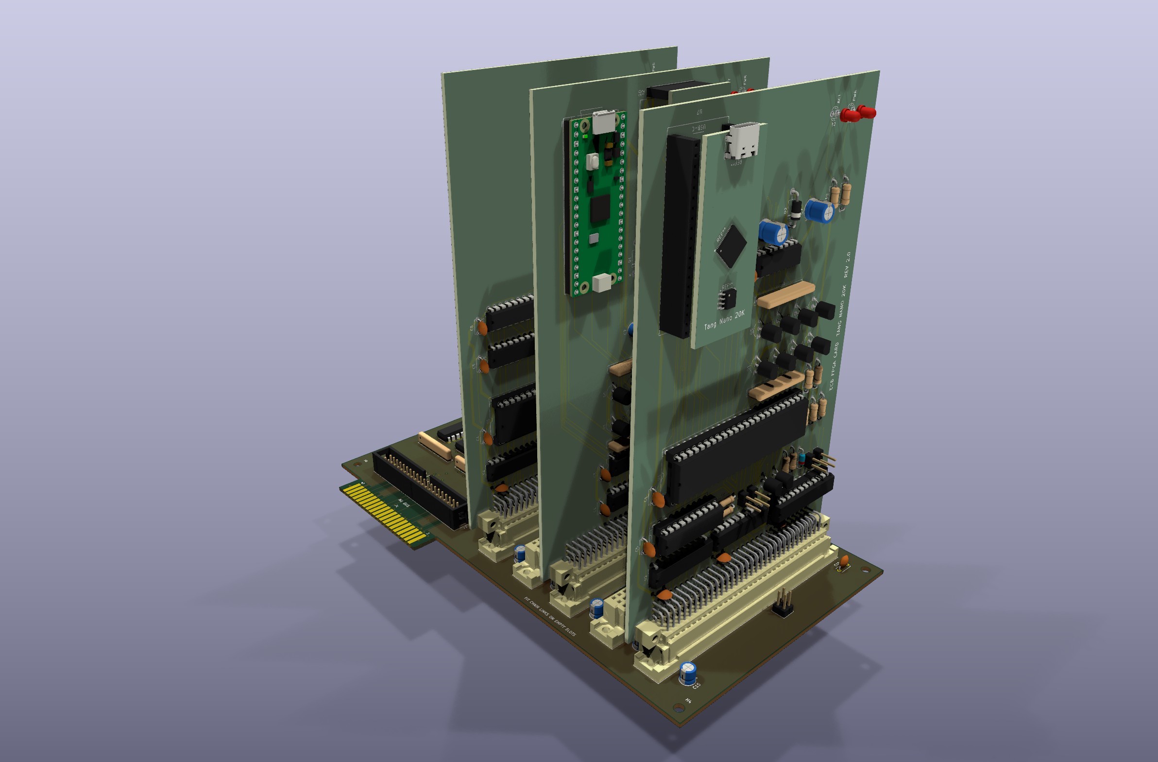
Main components on the Trs80 fpga card
Trs80 fpga card bill of materials (BOM)
52 components, 29 distinct parts.
| Qty | Part | Footprint | Refs |
|---|---|---|---|
| 1 | IDT7132SA/LA (2Kx8 DPRAM) | DIP-48_W15.24mm_Socket | U1 |
| 1 | 74HCT245 RAM<->BUS | DIP-20_W7.62mm | U2 |
| 1 | 74HCT245 PORT<->BUS | DIP-20_W7.62mm | U3 |
| 1 | ATF22V10C-15PU MEM_DECODE | DIP-24_W7.62mm_Socket | U4 |
| 1 | ATF16V8B-15PU IO_DECODE | DIP-20_W7.62mm_Socket | U5 |
| 1 | CD74HC4050E | DIP-16_W7.62mm | U6 |
| 1 | Tang Nano 9K | TangNano9K_DIP48_W22.86mm | U7 |
| 10 | 2N7000 | TO-92_Inline_Wide | Q1, Q2, Q3, Q4, Q5, Q6, Q7, Q8 +2 |
| 1 | M1 bus (card edge) | TRS80_M1_Edge_40 | J1 |
| 1 | To Expansion Interface | IDC-Header_2x20_P2.54mm_Vertical | J2 |
| 1 | 5V DC in | BarrelJack_Horizontal | J3 |
| 1 | FPGA spare I/O | PinHeader_2x08_P2.54mm_Vertical | J4 |
| 1 | BUSY->WAIT | PinHeader_1x02_P2.54mm_Vertical | JP1 |
| 1 | INT EN | PinHeader_1x02_P2.54mm_Vertical | JP2 |
| 1 | FULL 2K | PinHeader_1x02_P2.54mm_Vertical | JP3 |
| 1 | PORT ALT | PinHeader_1x02_P2.54mm_Vertical | JP4 |
| 1 | EDGE 5V | PinHeader_1x02_P2.54mm_Vertical | JP5 |
| 2 | 1N5819 | D_DO-41_SOD81_P10.16mm_Horizontal | D1, D2 |
| 1 | BAT85 | D_DO-35_SOD27_P7.62mm_Horizontal | D3 |
| 1 | ACT (green) | LED_D3.0mm | D4 |
Show 9 more
| Qty | Part | Footprint | Refs |
|---|---|---|---|
| 1 | PWR (red) | LED_D3.0mm | D5 |
| 6 | 100nF | C_Disc_D5.0mm_W2.5mm_P5.00mm | C1, C2, C3, C4, C5, C6 |
| 1 | 100uF 10V | CP_Radial_D6.3mm_P2.50mm | C7 |
| 1 | 10uF 10V | CP_Radial_D6.3mm_P2.50mm | C8 |
| 7 | 10k | R_Axial_DIN0207_L6.3mm_D2.5mm_P10.16mm_Horizontal | R1, R2, R5, R6, R7, R8, R9 |
| 2 | 4.7k | R_Axial_DIN0207_L6.3mm_D2.5mm_P10.16mm_Horizontal | R3, R4 |
| 1 | 470 | R_Axial_DIN0207_L6.3mm_D2.5mm_P10.16mm_Horizontal | R10 |
| 1 | 1k | R_Axial_DIN0207_L6.3mm_D2.5mm_P10.16mm_Horizontal | R11 |
| 2 | 4.7k | R_Array_SIP9 | RN1, RN2 |
Trs80 fpga card design files
The KiCad project lives in the davidellwood/trs80-m1-fpga-card repository on GitHub; these links point at the commit this page was built from.
Trs80 fpga card: common questions
How big is the Trs80 fpga card PCB?
The Trs80 fpga card measures 150 × 120 mm, has 2 copper layers and is 1.6 mm thick.
How many components are on the Trs80 fpga card?
52 components, from 29 distinct parts. The full bill of materials is listed on this page.
Where can I download the Trs80 fpga card design files?
From the davidellwood/trs80-m1-fpga-card repository on GitHub, which has the KiCad layout and the schematic; the links under Design files point to each one.
Can I use the Trs80 fpga card design in my own project?
Yes, under the terms of its MIT license, which davidellwood chose for the repository.
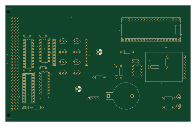
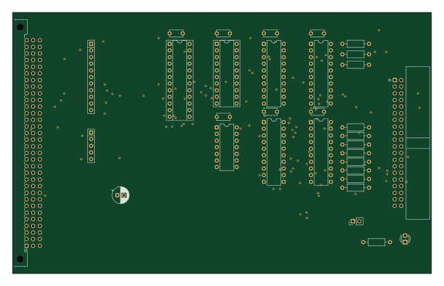
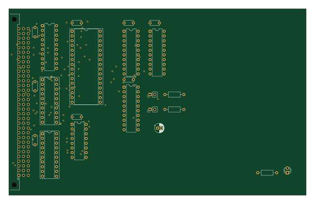
More boards in trs80-m1-fpga-card
Similar boards
Expansion Card Retrofit
FrameworkComputer
24 × 27.3 mm5 parts2LCC-BY-4.01.1k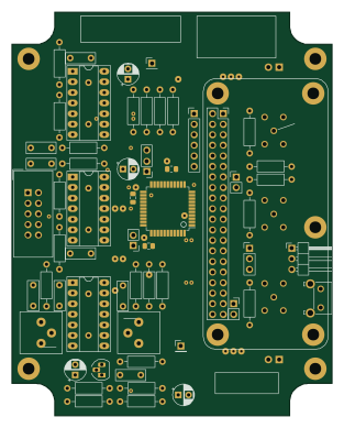
Rgb to hdmi
hoglet67
77 × 97 mm67 parts2LGPL-3.01.0k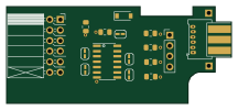
Buffer
53.9 × 23.2 mm13 parts2LGPL-3.01.0k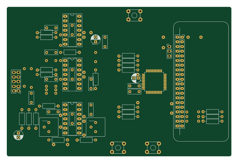
X1
121.9 × 81.3 mm51 parts2LGPL-3.01.0k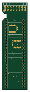
Amiga External
21.9 × 76.7 mm6 parts2LGPL-3.01.0k
Videoslotadapter
152 × 57.6 mm13 parts2LGPL-3.01.0k