
Hw trials

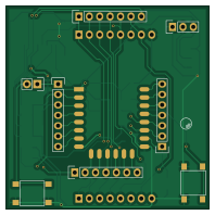
About the Hw trials PCB
Hw trials is an open source ESP8266 PCB design by forGGe, published on GitHub. It is a 2-layer board measuring 49.5 × 49.5 mm, with 28 components from 18 distinct parts.
Its main chip is the ESP-12E, from the ESP8266 family. Other key parts include the NCP1117ST33T3G. By type, the board carries 13 resistors, 7 connectors, 3 capacitors, 2 ICs, 2 switches and 1 jumper.
It belongs with the iot & wireless and displays & leds designs in this gallery.
From the project
A HW project made with help of KiCAD. Just for fun.
To use this project one should create symlink in home directory that points to project dir:
Main components on the Hw trials
Hw trials bill of materials (BOM)
28 components, 18 distinct parts — part numbers from the project's BOM.
| Qty | Part | Footprint | Refs |
|---|---|---|---|
| 1 | NCP1117ST33T3G | SOT-223 | U1 |
| 1 | ESP-12E | ESP-12E_with_3d | U2 |
| 1 | 0472192001 MICRO_SD_HINGE | MICRO_SD_HINGE_AMP | J2 |
| 3 | ESP_CONN | Pin_Header_Straight_1x07 | P1, P2, P3 |
| 1 | PWR_CONN | Pin_Header_Straight_1x03 | P4 |
| 1 | CONN_DISPLAY | Nokia_5110_LCD | P5 |
| 1 | SD_LCD_CONN | Pin_Header_Straight_1x07 | P6 |
| 1 | Jumper_NO_Small | Pin_Header_Straight_1x02 | JP1 |
| 1 | KEY_FLASH | SW_PUSH_SMD | SW1 |
| 1 | KEY_RST | SW_PUSH_SMD | SW2 |
| 1 | F920J107MBA 100uF | TantalC_SizeB_EIA-3528_Reflow | C1 |
| 1 | C0402C104K8PACTU 100nF | C_0402 | C2 |
| 1 | C0402C102K5RACTU 1nF | C_0402 | C3 |
| 1 | RC1206JR-07470RL 470 | R_1206 | R1 |
| 1 | RC1206JR-07220KL 220k | R_1206 | R2 |
| 1 | RC1206JR-07100KL 100k | R_1206 | R3 |
| 5 | RC1206JR-0712KL 12k | R_1206 | R6, R7, R8, R9, R10 |
| 5 | RC1206JR-0751KL 50k | R_1206 | R11, R12, R13, R14, R15 |
Hw trials design files
The KiCad project lives in the forGGe/hw_trials repository on GitHub; these links point at the commit this page was built from.
Hw trials: common questions
What microcontroller does the Hw trials use?
The Hw trials is built around the ESP-12E, from the ESP8266 family.
How big is the Hw trials PCB?
The Hw trials measures 49.5 × 49.5 mm, has 2 copper layers and is 1.6 mm thick.
How many components are on the Hw trials?
28 components, from 18 distinct parts, with part numbers taken from the project's own BOM. The full bill of materials is listed on this page.
Where can I download the Hw trials design files?
From the forGGe/hw_trials repository on GitHub, which has the KiCad layout and the BOM; the links under Design files point to each one.
Can I use the Hw trials design in my own project?
The repository has no license, so all rights stay with forGGe. Use it as a reference, and ask the author before reusing the design.
Can I test firmware for the Hw trials without the hardware?
Yes. HardLabs builds a simulation of the board from its netlist and BOM, so you can run and debug ESP8266 firmware against it before you order a PCB.
Similar boards
 ESP8266
ESP8266ControllerCircuit
stuartpittaway
75 × 30 mm20 parts2LCC-BY-NC-4.01.1k ESP8266
Duet WIFI
Duet3D
100 × 123 mm345 partsCERN-OHL-1.2257 ESP8266
RetroWiFiModem
mecparts
100 × 66.1 mm29 parts2LGPL-3.0256 ESP8266
Mideahvac dongle
reneklootwijk
20 × 48.5 mm19 parts2LNo license74 ESP8266
Single radio
AnyLeaf
37.7 × 37.7 mm43 parts4LMIT63 ESP8266
Esp8266-for uppatvind
horvathgergo
70 × 36 mm27 parts2LGPL-3.060