
UGC Main S1

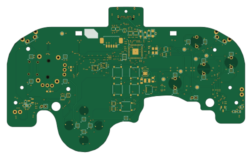
About the UGC Main S1 PCB
UGC Main S1 is an open source RP2040/RP2350 PCB design by HandHeldLegend, published on GitHub under the CC-BY-NC-4.0 license. It is a 4-layer board measuring 125.7 × 76.6 mm, with 121 components from 39 distinct parts.
Its main chip is the TPS63001DRCR, from the RP2040/RP2350 family. Other key parts include the LSM6DSRTR, USBLC6-2P6, TPS630001RCR, RP2040 and GD25Q80EEIGR. By type, the board carries 32 resistors, 25 capacitors, 18 inductors, 15 diodes, 10 switches and 8 ICs.
From the project
Resources Cross-Referenced for component placement and other spacing detail: - 3D Scans by Wesk - GCC CAD Model by GearHawk - PhobGCC PCB - 3D models for the ergonomic trigger reference were provided with full permission from YaBoiMikey

Main components on the UGC Main S1
UGC Main S1 bill of materials (BOM)
121 components, 39 distinct parts — part numbers from the project's BOM.
| Qty | Part | Footprint | Refs |
|---|---|---|---|
| 2 | LSM6DSRTR ST_LSM6 | LGA14 | U1, U2 |
| 1 | USBLC6-2P6 | SOT-666 | U3 |
| 1 | TPS630001RCR USBLC6-2P6 | SOT-666 | U4 |
| 1 | LSM6DSRTR USBLC6-2P6 | SOT-666 | U5 |
| 1 | TPS63001DRCR TPS630001RCR | VREG_V62_16624-01YE | U6 |
| 1 | RP2040 | QFN-56-1EP_7x7mm_P0.4mm_EP3.2x3.2mm | U7 |
| 1 | GD25Q80EEIGR | USON-8-EP(2x3) | U8 |
| 2 | BSS138DW-7-F BSS138DW | SOT-363_SC-70-6 | Q1, Q2 |
| 2 | MMBT2222A | SOT-23 | Q3, Q4 |
| 1 | ABM8-272-T3 | Crystal_SMD_3225-4Pin_3.2x2.5mm | Y1 |
| 1 | USB4056-03-A USB4056-03-A2 Global Connector Technology | USB405603A | J1 |
| 1 | 5051100792 Molex 5051100792 | CON_5051100792_MOL | J2 |
| 1 | PicoBlade_53261-0571 Conn_01x05_Socket Molex | Molex_PicoBlade_53261-0571_1x05-1MP_P1.25mm_Horizontal | J3 |
| 2 | SM02B-SURS-TF(LF)(SN) SM02B-SURS-TF_LF__SN_ | JST_SM02B-SURS-TF_LF__SN_ | J4, J5 |
| 2 | 5051100492 Conn_01x04_Socket | 5051100492 | J6, J9 |
| 1 | 5034800640 503480-0640 | 5034800640 | J10 |
| 1 | TMUX1204DQAR | TMUX1204DQAR | S1 |
| 1 | GL1807SYAE-002 GL18_SW | GL1807SYAE | SW1 |
| 6 | TS-1187A-C-E-B TS-1187A-C-A-B | TS-1187A-C-E-B | SW2, SW3, SW4, SW5, SW16, SW17 |
| 2 | TC-00100V H5.0 100gf SW_Push | Z_Switch_Edge_Omron | SW11, SW15 |
Show 19 more
| Qty | Part | Footprint | Refs |
|---|---|---|---|
| 6 | B5819WT M7C | D_SOD-523 | D1, D2, D3, D4, D5, D6 |
| 3 | CUS08F30,H3F | D_SOD-323_HandSoldering | D7, D8, D9 |
| 6 | BAS16VY,115 | SOT-363_SC-70-6 | D10, D11, D12, D13, D14, D15 |
| 17 | SK6805-EC-10 | SK6805-EC-10 | L1, L2, L3, L4, L5, L6, L7, L8 +9 |
| 1 | MIP25202R2MBE 1.3A 2.2uH ±20% 80mΩ | L_1008_2520Metric | L12 |
| 12 | CL03A104KQ3NNNC 100nF | C_0201_0603Metric | C1, C2, C5, C6, C7, C14, C15, C19 +4 |
| 2 | CC0603JRX7R9BB473 47nF | C_0603_1608Metric_Pad1.08x0.95mm_HandSolder | C3, C4 |
| 6 | GRM033R60J105KEA2D 1uF | C_0201_0603Metric | C8, C9, C10, C11, C16, C21 |
| 1 | TAJA476K006RNJ 47uF | CP_EIA-3216-18_Kemet-A | C12 |
| 2 | CL21A106KPFNNNE 10uF | C_0805_2012Metric | C13, C22 |
| 2 | CC0402FRNPO9BN150 15pF | C_0402_1005Metric | C17, C18 |
| 10 | RC0201FR-071KL 1k | R_0201_0603Metric | R1, R2, R3, R4, R5, R6, R7, R10 +2 |
| 2 | RC0201FR-075K1L 5.1k | R_0201_0603Metric | R8, R9 |
| 3 | RC0201FR-0710KL 10k | R_0201_0603Metric | R11, R12, R17 |
| 6 | RC0201FR-07100RL 100R | R_0201_0603Metric | R13, R14, R18, R23, R24, R25 |
| 4 | RC0201FR-070RL 0R | R_0201_0603Metric | R15, R16, R29, R30 |
| 5 | RC0201FR-0727RL 27R | R_0201_0603Metric | R19, R20, R26, R27, R28 |
| 1 | RC0201FR-07330RL 330R | R_0201_0603Metric | R21 |
| 1 | RC0402FR-07100KL 100k | R_0402_1005Metric | R32 |
UGC Main S1 design files
The KiCad project lives in the HandHeldLegend/GC-Ultimate repository on GitHub; these links point at the commit this page was built from.
UGC Main S1: common questions
What microcontroller does the UGC Main S1 use?
The UGC Main S1 is built around the TPS63001DRCR, from the RP2040/RP2350 family.
How big is the UGC Main S1 PCB?
The UGC Main S1 measures 125.7 × 76.6 mm, has 4 copper layers and is 1.6 mm thick.
How many components are on the UGC Main S1?
121 components, from 39 distinct parts, with part numbers taken from the project's own BOM. The full bill of materials is listed on this page.
Where can I download the UGC Main S1 design files?
From the HandHeldLegend/GC-Ultimate repository on GitHub, which has the KiCad layout, the schematic and the BOM; the links under Design files point to each one.
Can I use the UGC Main S1 design in my own project?
It is published under CC-BY-NC-4.0, which limits how it may be reused; read the license before building on it.
Can I test firmware for the UGC Main S1 without the hardware?
Yes. HardLabs builds a simulation of the board from its netlist and BOM, so you can run and debug RP2040/RP2350 firmware against it before you order a PCB.
More boards in GC-Ultimate
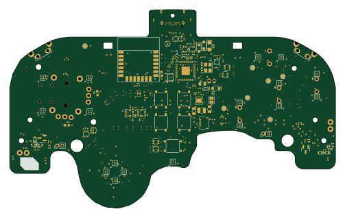
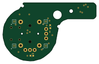

Similar boards
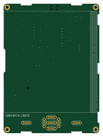 RP2040/RP2350
Open Book Abridged Edition
joeycastillo
85 × 115 mm29 parts2LCC-BY-SA-4.08.1k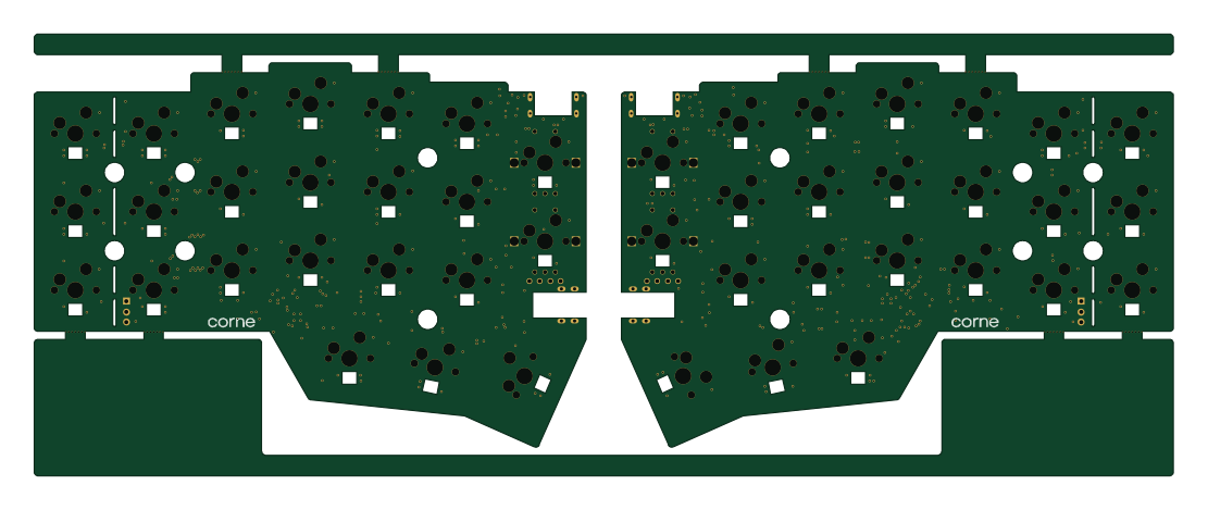 RP2040/RP2350
Corne
foostan
277.2 × 107.5 mm164 parts2LCC-BY-4.07.7k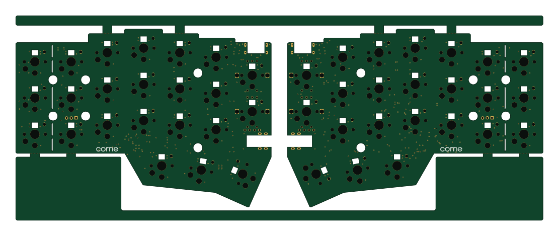 RP2040/RP2350
Corne
277.2 × 107.5 mm164 parts2LCC-BY-4.07.7k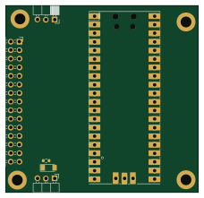 RP2040/RP2350
LogicAnalyzer
gusmanb
57 × 55.2 mm6 parts2LGPL-3.05.0k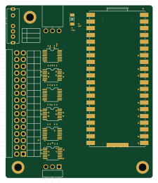 RP2040/RP2350
Jitx design
55.5 × 65 mm26 parts4LGPL-3.05.0k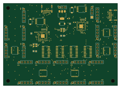 RP2040/RP2350
Main
google
98 × 71 mm102 parts2LApache-2.02.9k