
KS-Hauptsignal


About the KS-Hauptsignal PCB
KS-Hauptsignal is an open source PCB design by jgraichen, published on GitHub under the CC-BY-SA-4.0 license. It is a 2-layer board measuring 6.6 × 13.6 mm, with 8 components from 4 distinct parts.
From the project
This work is licensed under a Creative Commons Attribution-ShareAlike 4.0 International License.
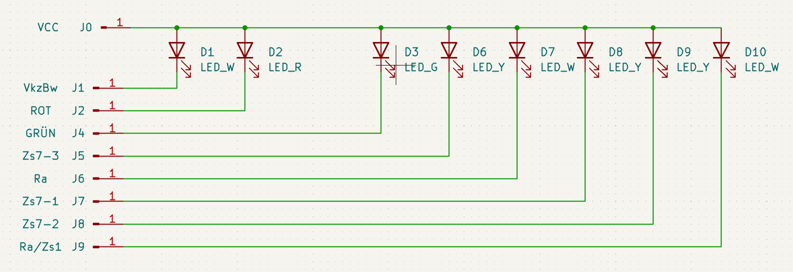
KS-Hauptsignal bill of materials (BOM)
8 components, 4 distinct parts.
| Qty | Part | Footprint | Refs |
|---|---|---|---|
| 3 | LED_W | LED_0402_1005Metric | D1, D7, D10 |
| 1 | LED_R | LED_0402_1005Metric | D2 |
| 1 | LED_G | LED_0402_1005Metric | D3 |
| 3 | LED_Y | LED_0402_1005Metric | D6, D8, D9 |
KS-Hauptsignal design files
The KiCad project lives in the jgraichen/railway-signals repository on GitHub; these links point at the commit this page was built from.
KS-Hauptsignal: common questions
How big is the KS-Hauptsignal PCB?
The KS-Hauptsignal measures 6.6 × 13.6 mm, has 2 copper layers and is 0.8 mm thick.
How many components are on the KS-Hauptsignal?
8 components, from 4 distinct parts. The full bill of materials is listed on this page.
Where can I download the KS-Hauptsignal design files?
From the jgraichen/railway-signals repository on GitHub, which has the KiCad layout and the schematic; the links under Design files point to each one.
Can I use the KS-Hauptsignal design in my own project?
Yes, under the terms of its CC-BY-SA-4.0 license, which jgraichen chose for the repository.
More boards in railway-signals
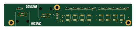
WS2811 LED Driver 24 (2 Signals)
140 × 25 mm16 parts2LCC-BY-SA-4.01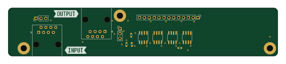
WS2811 LED Driver 12 (1 Signal)
140 × 25 mm12 parts2LCC-BY-SA-4.01
MS
6.6 × 13.6 mm9 parts2LCC-BY-SA-4.01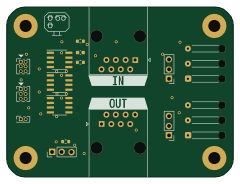
WS2811 LED Driver 9LS (2 Lichtsperrsignal)
60 × 45 mm8 parts2LCC-BY-SA-4.01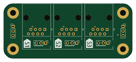
MGP Decoder adapter board to RJ45 loop
70 × 30 mm8 parts2LCC-BY-SA-4.01
KS-Signalschirm für mehrfarbige Optik
6.6 × 13.6 mm7 parts2LCC-BY-SA-4.01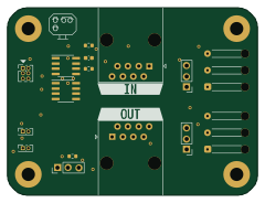
WS2811 LED Driver 6LS (1 Lichtsperrsignal)
60 × 45 mm7 parts2LCC-BY-SA-4.01
KS-Vorsignal
6.6 × 10.8 mm4 parts2LCC-BY-SA-4.01