
Receiver effects

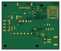
About the Receiver effects PCB
Receiver effects is an open source PCB design by JMET04, published on GitHub under the MIT license. It is a 4-layer board measuring 50.3 × 42.3 mm, with 14 components from 14 distinct parts.
Other key parts include the NINA-B302-00B-00, TPS62162DSGR, USBLC6-2SC6 and MAX98357AETE+T. By type, the board carries 4 ICs, 3 connectors, 1 transistor, 1 fuse, 1 diode and 1 inductor.
It belongs with the audio designs in this gallery.
From the project
Deterministic CAD/EDA agent plugin for 2D drawings, AutoCAD, SolidWorks, KiCad, review gates and auditable delivery.
Status: design input only; fabrication is blocked.
This is the independent media receiver direction. It is intentionally separate from both the existing receiver baseline and the wand order. It contains only the NINA-B302 radio/MCU concept, protected 5 V / 2 A USB-C input, 3.3 V logic, an 8-pin GC9A01A module interface, MAX98357A I2S amplifier with differential 4 ohm speaker connector, and a discrete 3.3 V RGB status LED. Legacy UART, optocoupler and 12 V MOSFET actuator channels are not copied.
Main components on the Receiver effects
Receiver effects bill of materials (BOM)
14 components, 14 distinct parts — part numbers from the project's BOM.
| Qty | Part | Footprint | Refs |
|---|---|---|---|
| 1 | NINA-B302-00B-00 u-blox | receiver-effects_U1 | U1 |
| 1 | TPS62162DSGR Texas Instruments | receiver-effects_U2 | U2 |
| 1 | USBLC6-2SC6 STMicroelectronics | receiver-effects_U3 | U3 |
| 1 | MAX98357AETE+T Analog Devices | receiver-effects_U4 | U4 |
| 1 | AO3401A Alpha & Omega Semiconductor | receiver-effects_Q1 | Q1 |
| 1 | DX07S016JA1R1500 USB-C 5V INPUT JAE | receiver-effects_J1 | J1 |
| 1 | SM08B-GHS-TB(LF)(SN) GC9A01A 1.28in SPI JST | receiver-effects_J2 | J2 |
| 1 | S2B-PH-SM4-TB(LF)(SN) 4OHM BTL SPEAKER JST | receiver-effects_J3 | J3 |
| 1 | GRM21BR61A106KE19L 10uF 10V X5R Murata | receiver-effects_C_AUDIO_10U | C_AUDIO_10U |
| 1 | MF-MSMF150-2 1.5A PTC Bourns | receiver-effects_F1 | F1 |
| 1 | RC0402FR-075K1L 5.1k Yageo | receiver-effects_R_CC1 | R_CC1 |
| 1 | RC0402FR-075K1L 5.1k Yageo | receiver-effects_R_CC2 | R_CC2 |
| 1 | LTST-C19HE1WT RGB COMMON ANODE Lite-On | receiver-effects_D1 | D1 |
| 1 | LQH32PN2R2NN0L 2.2uH Murata | receiver-effects_L1 | L1 |
Receiver effects design files
The KiCad project lives in the JMET04/aicad-agent repository on GitHub; these links point at the commit this page was built from.
Receiver effects: common questions
How big is the Receiver effects PCB?
The Receiver effects measures 50.3 × 42.3 mm, has 4 copper layers and is 1.6 mm thick.
How many components are on the Receiver effects?
14 components, from 14 distinct parts, with part numbers taken from the project's own BOM. The full bill of materials is listed on this page.
Where can I download the Receiver effects design files?
From the JMET04/aicad-agent repository on GitHub, which has the KiCad layout, the schematic and the BOM; the links under Design files point to each one.
Can I use the Receiver effects design in my own project?
Yes, under the terms of its MIT license, which JMET04 chose for the repository.
More boards in aicad-agent
Similar boards
KLOR
GEIGEIGEIST
160.2 × 118.3 mm79 parts2LGPL-3.01.2k
ButtonsLEDs
shanteacontrols
390 × 37 mm82 parts2LApache-2.0956
USB
52 × 12.6 mm6 parts2LApache-2.0956
Pots
390 × 93 mm75 parts2LApache-2.0956
PicoGUS Hand386
polpo
29.2 × 75.2 mm43 parts4LGPL-2.0800
Snark barker
schlae
231.1 × 106.7 mm193 parts2LNo license687