
Splitter

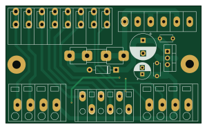
About the Splitter PCB
Splitter is an open source PCB design by kwiecinski, published on GitHub under the MIT license. It is a 2-layer board measuring 75 × 45 mm, with 12 components from 11 distinct parts.
Other key parts include the L7812. By type, the board carries 5 connectors, 4 capacitors, 1 IC, 1 fuse and 1 diode.
It belongs with the iot & wireless, power & battery and sensors designs in this gallery.
From the project
Project contains BMS for lead-acid batteries and ESP-based board used to pull information from EASUN offgrid inverter, energy meters and sensors. It show informations od displays and use ESPhome to send it to Home Assistant..
1. Photovoltaic modules 2. Concrete base mounting 3. Metalworking and welding mounting bases and angle bar 4. Painting mounting base, angle bars and perforated profiles 5. PV mountings to perforated profiles 6. Assembly of PV installation 7. Fully assembled PV installation 8. Underground Cable Installation and Connection to the Building
B. EASUN inverter - description, installation schematic and wiring #### C. Managemenet system part: - BMS for lead-acid batteries - equalize battery, protect from large charge/discharge currents, montors battery state (temp, voltage) - ESP32 Master module -…
Main components on the Splitter
Splitter bill of materials (BOM)
12 components, 11 distinct parts — part numbers from the project's BOM.
| Qty | Part | Footprint | Refs |
|---|---|---|---|
| 1 | L7812 | TO-220-3_Vertical | U1 |
| 1 | SIGNAL_TERMINAL | WAGO-255-8P | J2 |
| 1 | DIODE_PROBE | WAGO-739-4P | J6 |
| 1 | OPTICAL_PROBE | HDQ-250-6P | J7 |
| 1 | UNUSED | WAGO-739-4P | J8 |
| 1 | POWER_SUPPLY | Screw-Terminal-P6-rast-5mm-6,7x30 | J11 |
| 1 | Fuse | Fuseholder_Clip-5x20mm_Eaton_1A5601-01_Inline_P20.80x6.76mm_D1.70mm_Horizontal | F1 |
| 1 | LL4148 1N4007 | D_DO-41_SOD81_P10.16mm_Horizontal | D1 |
| 1 | 1000u/35V | CP_Radial_D10.0mm_P5.00mm | C1 |
| 2 | 100n | C_Disc_D4.7mm_W2.5mm_P5.00mm | C2, C3 |
| 1 | 100u/16V | CP_Radial_D6.3mm_P2.50mm | C4 |
Splitter design files
The KiCad project lives in the kwiecinski/BMS-and-offgrid-photovoltaic-management-system repository on GitHub; these links point at the commit this page was built from.
Splitter: common questions
How big is the Splitter PCB?
The Splitter measures 75 × 45 mm, has 2 copper layers and is 1.6 mm thick.
How many components are on the Splitter?
12 components, from 11 distinct parts, with part numbers taken from the project's own BOM. The full bill of materials is listed on this page.
Where can I download the Splitter design files?
From the kwiecinski/BMS-and-offgrid-photovoltaic-management-system repository on GitHub, which has the KiCad layout, the schematic and the BOM; the links under Design files point to each one.
Can I use the Splitter design in my own project?
Yes, under the terms of its MIT license, which kwiecinski chose for the repository.
More boards in BMS-and-offgrid-photovoltaic-management-system
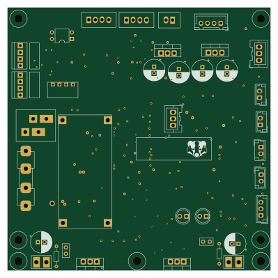
Balancer
99.5 × 99.5 mm165 parts2LMIT3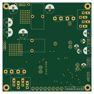 PIC
PICBidirectional Power Converter 24V-12V with BMS
99.5 × 99.5 mm156 parts2LMIT3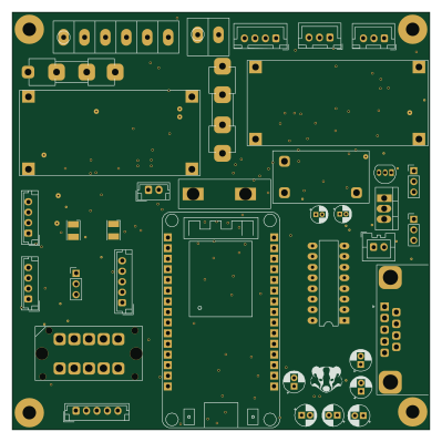 ESP32
ESP32ESP32 master
99.5 × 99.5 mm153 parts2LMIT3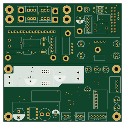 PIC
PICMisc
99.5 × 99.5 mm152 parts2LMIT3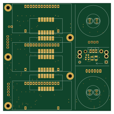
DC line module+Meter probe
100 × 100 mm98 parts2LMIT3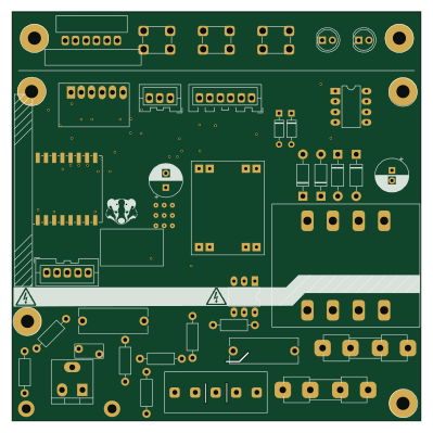
Power tracking heaterP
99.5 × 99.5 mm74 parts2LMIT3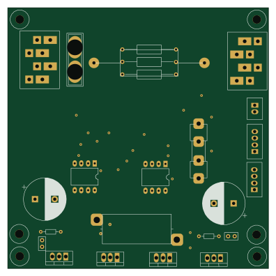
Current-Limiter
99 × 99 mm62 parts2LMIT3
Similar boards
Sensor smd
scottbez1
40 × 20 mm5 parts2LApache-2.04.2k
Sensors
StuckAtPrototype
15.2 × 9 mm14 parts4LApache-2.03.8k
Stack chan
stack-chan
50 × 50 mm33 parts2LApache-2.01.7k
Display Carrier
AxxAxx
35.6 × 58.2 mm5 parts2LGPL-3.01.7k
Microphone
Mentra-Community
5.5 × 6.1 mm6 parts2LMIT1.2k
Module 16S PassiveBalanceAddOn
stuartpittaway
61 × 74 mm86 parts2LCC-BY-NC-4.01.1k