
LED


About the LED PCB
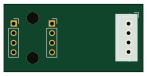
LED is an open source PCB design by markantosa, published on GitHub. It is a 2-layer board measuring 15.9 × 17.2 mm, with 3 components from 3 distinct parts.
By type, the board carries 1 connector, 1 diode and 1 resistor.
It belongs with the robotics & motion designs in this gallery.
From the project
[SUTD 30.007] Embolisation agent characterisation and automated mixing system
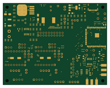
KiCad schematic and PCB layout for the EMBO ESP32-S3 control board.
Current fabricated/in-progress revision: v3.4 (hardware/electrical/embo main MCU PCB v34/). The prior embo main MCU PCB v25/ folder is kept for reference only — see below for what changed between them.
Full design specification, component values, GPIO assignments, layout rules, BOM, and pre-submission checklist: /docs/EMBOPCBDesignBriefv34.txt`
LED bill of materials (BOM)
3 components, 3 distinct parts — part numbers from the project's BOM.
| Qty | Part | Footprint | Refs |
|---|---|---|---|
| 1 | Conn_01x02 | JST_XH_B2B-XH-A_1x02_P2.50mm_Vertical | J1 |
| 1 | BAV99 LED | LED_D5.0mm | D1 |
| 1 | R | R_Axial_DIN0207_L6.3mm_D2.5mm_P10.16mm_Horizontal | R1 |
LED design files
The KiCad project lives in the markantosa/embo repository on GitHub; these links point at the commit this page was built from.
LED: common questions
How big is the LED PCB?
The LED measures 15.9 × 17.2 mm, has 2 copper layers and is 1.6 mm thick.
How many components are on the LED?
3 components, from 3 distinct parts, with part numbers taken from the project's own BOM. The full bill of materials is listed on this page.
Where can I download the LED design files?
From the markantosa/embo repository on GitHub, which has the KiCad layout, the schematic and the BOM; the links under Design files point to each one.
Can I use the LED design in my own project?
The repository has no license, so all rights stay with markantosa. Use it as a reference, and ask the author before reusing the design.
More boards in embo

Similar boards
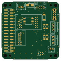
Stack chan
stack-chan
50 × 50 mm33 parts2LApache-2.01.7k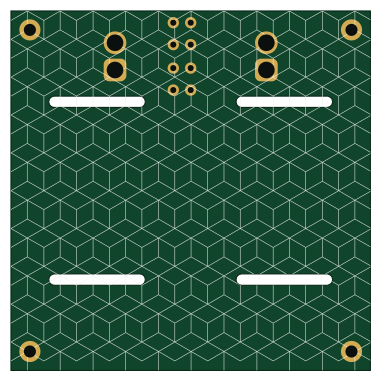
Cube batteryboard
willem-pennings
95 × 95 mm4 parts2LGPL-3.01.1k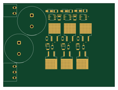
Trollerv2
rene-dev
100 × 75 mm33 parts4LGPL-3.0979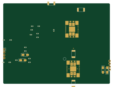
Powerstep
95.2 × 71.5 mm28 parts4LGPL-3.0979
11ua
57.3 × 19 mm26 parts2LGPL-3.0979
Diff driver
32 × 22 mm14 parts2LGPL-3.0979