
Parte2

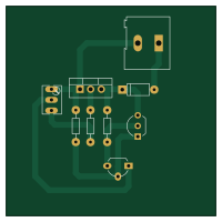
About the Parte2 PCB
Parte2 is an open source PCB design by MyCloudExample, published on GitHub. It is a 2-layer board measuring 50 × 50 mm, with 9 components from 9 distinct parts.
Other key parts include the LM317L_TO92 and LM35-LP. By type, the board carries 3 resistors, 2 ICs, 1 transistor and 1 diode.
Main components on the Parte2
Parte2 bill of materials (BOM)
9 components, 9 distinct parts.
| Qty | Part | Footprint | Refs |
|---|---|---|---|
| 1 | LM317L_TO92 | TO-220-3_Vertical | U1 |
| 1 | LM35-LP | TO-92_Molded_Wide_Oval | U2 |
| 1 | BC557 | TO-92_Inline_Wide | Q1 |
| 1 | — | TerminalBlock_Altech_AK300-2_P5.00mm | Entrada_Sensor1 |
| 1 | 100 | Potentiometer_Trimmer_Bourns_3266Y | RV1 |
| 1 | 1N5819 | D_A-405_P7.62mm_Horizontal | D1 |
| 1 | 4k7 | R_Axial_DIN0204_L3.6mm_D1.6mm_P7.62mm_Horizontal | R2 |
| 1 | 560 | R_Axial_DIN0204_L3.6mm_D1.6mm_P7.62mm_Horizontal | R5 |
| 1 | 62,5 | R_Axial_DIN0204_L3.6mm_D1.6mm_P7.62mm_Horizontal | R8 |
Parte2 design files
The KiCad project lives in the MyCloudExample/Kicad_Proyectos repository on GitHub; these links point at the commit this page was built from.
Parte2: common questions
How big is the Parte2 PCB?
The Parte2 measures 50 × 50 mm, has 2 copper layers and is 1.6 mm thick.
How many components are on the Parte2?
9 components, from 9 distinct parts. The full bill of materials is listed on this page.
Where can I download the Parte2 design files?
From the MyCloudExample/Kicad_Proyectos repository on GitHub, which has the KiCad layout; the links under Design files point to each one.
Can I use the Parte2 design in my own project?
The repository has no license, so all rights stay with MyCloudExample. Use it as a reference, and ask the author before reusing the design.
More boards in Kicad_Proyectos
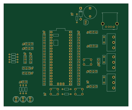 RP2040/RP2350
Placa de Desarrollo
115 × 95 mm44 parts2LNo license1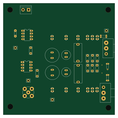
Oscilador 555
100 × 100 mm40 parts2LNo license1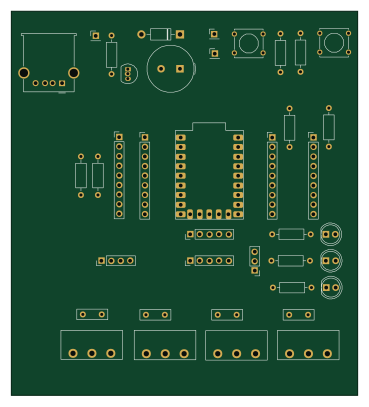 RP2040/RP2350
Placa de desarrollo Pico Zero
91.5 × 101.6 mm39 parts2LNo license1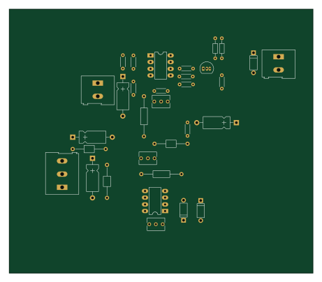
AMPLIFICADOR DE TERMO J COMPENSADO
115 × 100 mm32 parts2LNo license1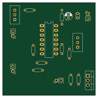
Ampli de Celda de Carga
50 × 50 mm19 parts2LNo license1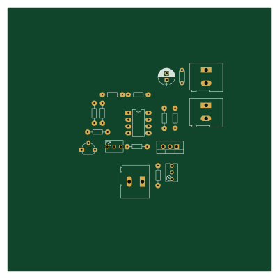
PT100
100 × 100 mm17 parts2LNo license1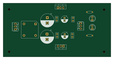
FUENTE SIMETRICA DE 12V
100 × 50 mm17 parts2LNo license1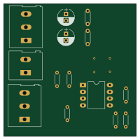
Receptor
50 × 50 mm14 parts2LNo license1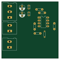
Transmisor
50 × 50 mm14 parts2LNo license1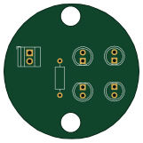
Linterna Leds
40.1 × 40.1 mm6 parts2LNo license1