
Fpga gpu

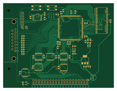
About the Fpga gpu PCB
Fpga gpu is an open source FPGA PCB design by nojan1, published on GitHub. It is a 2-layer board measuring 99.3 × 76 mm, with 67 components from 25 distinct parts.
Its main chip is the ICE40HX4K-TQ144, from the FPGA family. Other key parts include the SST25VF080B-50-4x-S2Ax, 74HCT541, TXS0108EPW, AMS1117-3.3 and AP2112K-1.2. By type, the board carries 24 capacitors, 16 resistors, 11 ICs, 8 jumpers, 3 connectors and 2 switches.
From the project
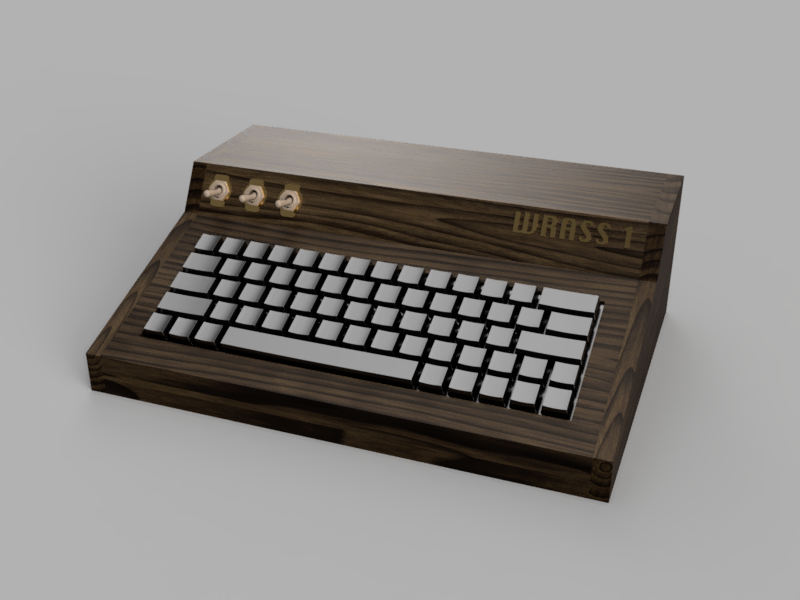
The purpose of Project Wrass is to develop the Wrass 1.
The purpose of Project Wrass is to develop the Wrass 1.
A 6502 based computer having the following specs.
W65C02 running at 2Mhz Bankable RAM giving a total of approx 300KB of usable memory * Expansion bus for up to 16 devices
The 16KB ROM is bankable using an external switch. This allows the computer to run "2 sets" of software.
The existing one is a simple homebrew "monitor" giving access to simple read, write and jump commands.
Main components on the Fpga gpu
Fpga gpu bill of materials (BOM)
67 components, 25 distinct parts.
| Qty | Part | Footprint | Refs |
|---|---|---|---|
| 1 | ICE40HX4K-TQ144 | TQFP-144_20x20mm_P0.5mm | U1 |
| 1 | SST25VF080B-50-4x-S2Ax | SOIC-8_5.275x5.275mm_P1.27mm | U2 |
| 3 | 74HCT541 | SSOP-20_4.4x6.5mm_P0.65mm | U3, U4, U5 |
| 2 | TXS0108EPW | TSSOP-20_4.4x6.5mm_P0.65mm | U6, U7 |
| 1 | AMS1117-3.3 | SOT-223-3_TabPin2 | U8 |
| 1 | AP2112K-1.2 | SOT-23-5 | U9 |
| 1 | IS61C5128AL-10KLI | SOJ-36_10.16x23.49mm_P1.27mm | U10 |
| 1 | 74HCT00 | SSOP-14_5.3x6.2mm_P0.65mm | U11 |
| 1 | 2N7002 | SOT-23 | Q1 |
| 1 | TXC-7C | Oscillator_SMD_TXC_7C-4Pin_5.0x3.2mm | X1 |
| 1 | Bus expansion | PinHeader_2x20_P2.54mm_Horizontal | J2 |
| 1 | programming | PinHeader_1x06_P2.54mm_Vertical | J3 |
| 1 | reset ground | PinHeader_1x01_P2.54mm_Vertical | J4 |
| 8 | SolderJumper_2_Open | SolderJumper-2_P1.3mm_Open_RoundedPad1.0x1.5mm | JP1, JP2, JP3, JP4, JP5, JP6, JP7, JP8 |
| 1 | SW_Reset | SW_SPST_TL3305A | SW1 |
| 1 | SW_FlashPwrCycle | SW_SPST_TL3305A | SW2 |
| 1 | 1N5817 | D_0805_2012Metric | D1 |
| 19 | 100n | C_0805_2012Metric | C1, C2, C3, C4, C5, C6, C7, C8 +11 |
| 1 | 100nf | C_Radial_D5.0mm_H7.0mm_P2.00mm | C18 |
| 4 | 22u | C_0805_2012Metric | C19, C20, C21, C22 |
Show 5 more
| Qty | Part | Footprint | Refs |
|---|---|---|---|
| 2 | 22R | R_0805_2012Metric | R1, R5 |
| 5 | 10k | R_0805_2012Metric | R2, R3, R4, R15, R16 |
| 3 | 470 | R_0805_2012Metric | R6, R9, R12 |
| 3 | 1k | R_0805_2012Metric | R7, R10, R13 |
| 3 | 1k8 | R_0805_2012Metric | R8, R11, R14 |
Fpga gpu design files
The KiCad project lives in the nojan1/project-wrass repository on GitHub; these links point at the commit this page was built from.
Fpga gpu: common questions
What microcontroller does the Fpga gpu use?
The Fpga gpu is built around the ICE40HX4K-TQ144, from the FPGA family.
How big is the Fpga gpu PCB?
The Fpga gpu measures 99.3 × 76 mm, has 2 copper layers and is 1.6 mm thick.
How many components are on the Fpga gpu?
67 components, from 25 distinct parts. The full bill of materials is listed on this page.
Where can I download the Fpga gpu design files?
From the nojan1/project-wrass repository on GitHub, which has the KiCad layout and the schematic; the links under Design files point to each one.
Can I use the Fpga gpu design in my own project?
The repository has no license, so all rights stay with nojan1. Use it as a reference, and ask the author before reusing the design.
Can I test firmware for the Fpga gpu without the hardware?
Yes. HardLabs builds a simulation of the board from its netlist and BOM, so you can run and debug FPGA firmware against it before you order a PCB.
More boards in project-wrass
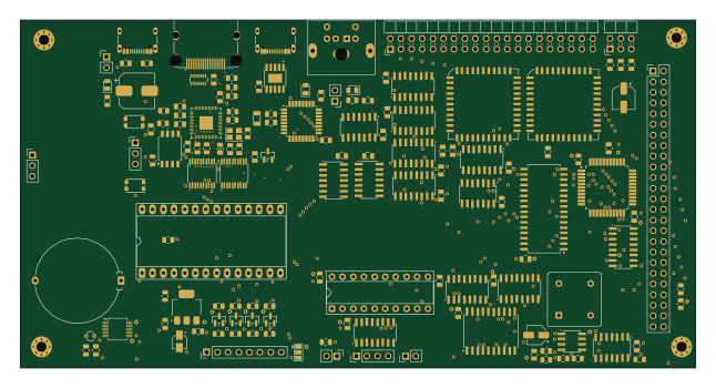 RP2040/RP2350
All in one smc
161.1 × 82.9 mm146 parts4LNo license0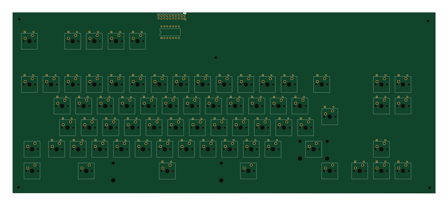
Keyboard
372.1 × 159.1 mm136 parts2LNo license0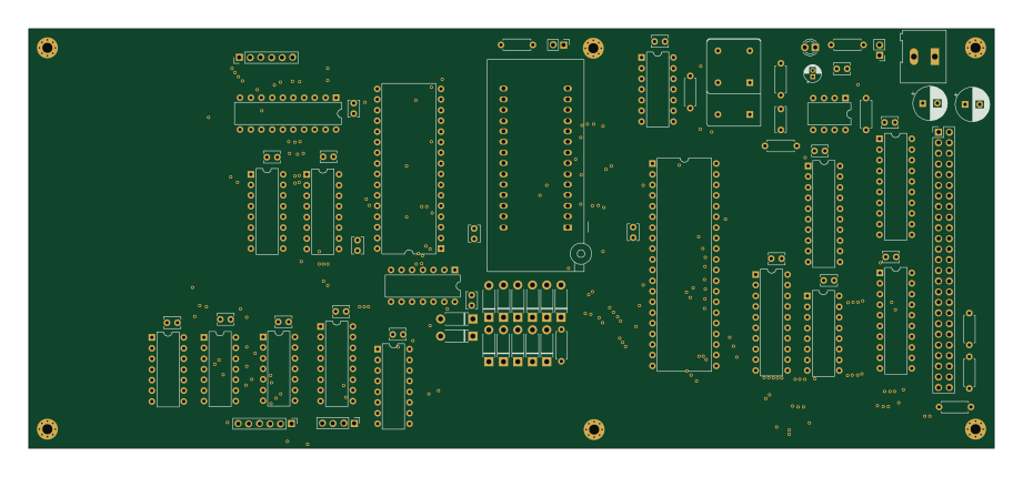
Main board
230 × 100 mm74 parts4LNo license0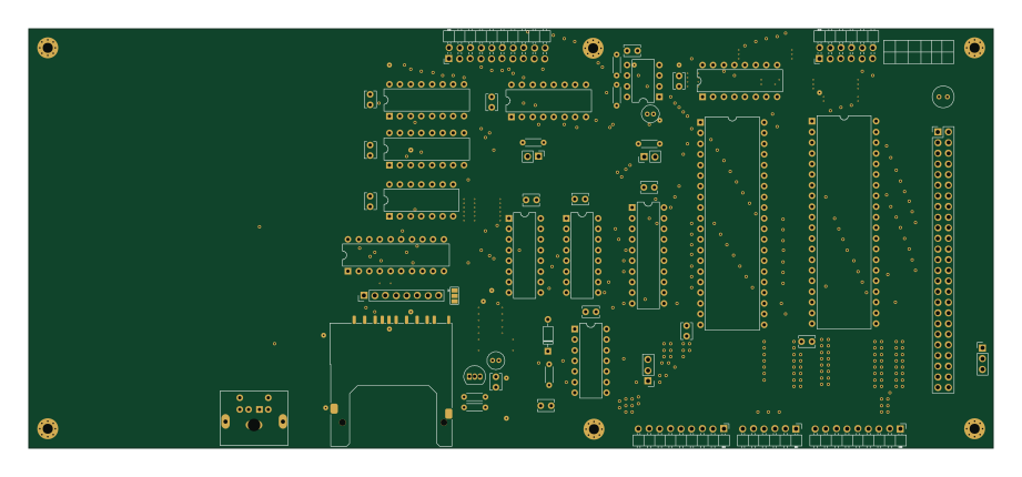
Io card
230 × 100 mm61 parts2LNo license0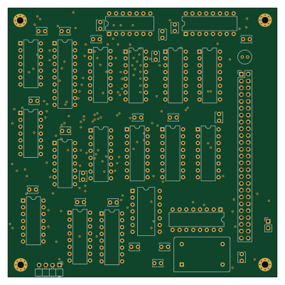
Uart
100 × 100 mm53 parts4LNo license0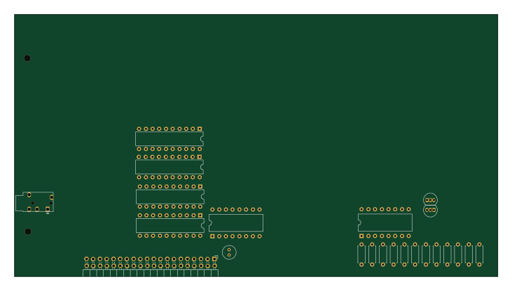
Audio card
182.4 × 99.1 mm31 parts2LNo license0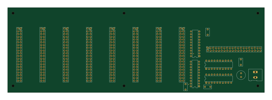
Expansion backplane
235.7 × 78.5 mm19 parts2LNo license0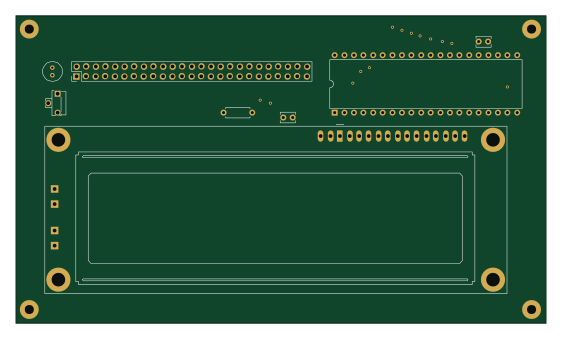
Lcd interface
140.2 × 81.3 mm16 parts2LNo license0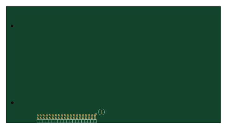
Expansion skeleton
182.4 × 99.1 mm10 parts2LNo license0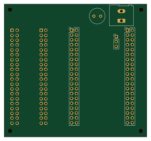
Expansion breakout
73.9 × 69 mm7 parts2LNo license0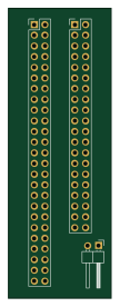
Expansion-40-to-50-conversion
24.4 × 68.8 mm3 parts2LNo license0
Similar boards
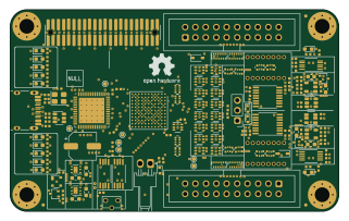 FPGA
Base board
GlasgowEmbedded
80 × 49 mm222 parts4L0BSD2.2k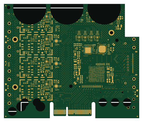 FPGA
Thunderscope Rev5.3
EEVengers
122.5 × 103.5 mm817 parts6LMIT1.3k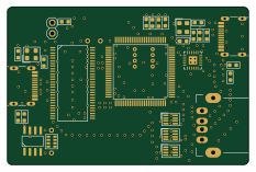 FPGA
Usb sniffer
ataradov
58.2 × 38.1 mm86 parts2LBSD-3-Clause1.3k FPGA
Tomu, I'm
theacodes
13 × 9.4 mm40 parts4LMIT1.1k FPGA
Icepi zero
cheyao
65 × 30 mm143 parts4LSHL-2.1828 FPGA
Gcvideo
ikorb
49 × 30 mm44 parts4LNo license765