
In13-nixie device

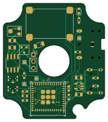
About the In13-nixie device PCB
In13-nixie device is an open source ESP32 PCB design by nonik0, published on GitHub. It is a 2-layer board measuring 38.1 × 43.1 mm, with 29 components from 20 distinct parts.
Its main chip is the ESP32-C6-MINI-1/U, from the ESP32 family. Other key parts include the LM358, AP2112K-3.3 and HV Module. By type, the board carries 10 resistors, 5 connectors, 5 capacitors, 4 ICs, 2 switches and 1 transistor.
It belongs with the displays & leds designs in this gallery.
From the project
This Nixie project is a continutation of the same spirit of most of my earlier Nixie projects: take an existing Nixie device, house it in a clean, well-built metal case, and maybe do a few addtions or modifications along the way. For me, the magic of Nixie tubes lies in their sof
This Nixie project is a continutation of the same spirit of most of my earlier Nixie projects: take an existing Nixie device, house it in a clean, well-built metal case, and maybe do a few addtions or modifications along the way. For me, the magic of Nixie tubes lies in their soft, ghostly glow—subtle, warm, and inviting. A simple, high-quality enclosure helps keep the attention where it belongs: on the Nixie itself.
Main components on the In13-nixie device
In13-nixie device bill of materials (BOM)
29 components, 20 distinct parts.
| Qty | Part | Footprint | Refs |
|---|---|---|---|
| 1 | LM358 | SOIC-8_3.9x4.9mm_P1.27mm | U1 |
| 1 | ESP32-C6-MINI-1/U | ESP32-C6-MINI-1U | U2 |
| 1 | AP2112K-3.3 | SOT-23-5 | U4 |
| 1 | HV Module | AliExpress_HV_Module | U11 |
| 1 | MMBTA42 | SOT-23 | Q1 |
| 1 | PINHD_1x3_Female | PinSocket_1x03_P2.54mm_Vertical | J1 |
| 1 | AudioJack3 | Jack_3.5mm_CUI_SJ1-3523N_Horizontal_NoEdgeSilkscreen | J2 |
| 1 | USB_C_Receptacle_USB2.0_16P | USB_C_Receptacle_HCTL_HC-TYPE-C-16P-01A | J3 |
| 2 | PINHD_1x4_Male | Pads_1x4_2.54mm | J4, J5 |
| 1 | 2k | Potentiometer_Bourns_TC33X_Vertical | RV1 |
| 2 | SW_Push | Mitsumi_SOFSeries_SMD_Button | SW1, SW2 |
| 1 | LED | LED_0603_1608Metric | D3 |
| 1 | 100nF | C_0805_2012Metric | C2 |
| 2 | 1u | C_0603_1608Metric | C3, C4 |
| 2 | 22u | C_0805_2012Metric | C9, C12 |
| 1 | 220k | R_1206_3216Metric | R1 |
| 5 | 10k | R_0603_1608Metric | R2, R3, R5, R6, R11 |
| 1 | 330 | R_0805_2012Metric | R4 |
| 2 | 5.1K | R_0603_1608Metric | R12, R13 |
| 1 | 220 | R_0603_1608Metric | R14 |
In13-nixie device design files
The KiCad project lives in the nonik0/in13-nixie-device repository on GitHub; these links point at the commit this page was built from.
In13-nixie device: common questions
What microcontroller does the In13-nixie device use?
The In13-nixie device is built around the ESP32-C6-MINI-1/U, from the ESP32 family.
How big is the In13-nixie device PCB?
The In13-nixie device measures 38.1 × 43.1 mm, has 2 copper layers and is 1.6 mm thick.
How many components are on the In13-nixie device?
29 components, from 20 distinct parts. The full bill of materials is listed on this page.
Where can I download the In13-nixie device design files?
From the nonik0/in13-nixie-device repository on GitHub, which has the KiCad layout and the schematic; the links under Design files point to each one.
Can I use the In13-nixie device design in my own project?
The repository has no license, so all rights stay with nonik0. Use it as a reference, and ask the author before reusing the design.
Can I test firmware for the In13-nixie device without the hardware?
Yes. HardLabs builds a simulation of the board from its netlist and BOM, so you can run and debug ESP32 firmware against it before you order a PCB.
Similar boards
 ESP32
OSO-BOOK-B1
joeycastillo
85 × 115 mm65 parts2LCC-BY-SA-4.08.1k ESP32
Powertrain
byrantech
64 × 45.4 mm171 parts4LMIT4.3k ESP32
Badge
atopile
56.3 × 39 mm239 parts4LMIT4.0k ESP32
Esp32 minimal
36.2 × 26.8 mm20 parts2LMIT4.0k ESP32
Racer
StuckAtPrototype
36 × 50.2 mm70 parts4LApache-2.03.8k ESP32
Controller
29 × 74 mm58 parts4LApache-2.03.8k