
Ethernet

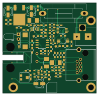
About the Ethernet PCB
Ethernet is an open source PCB design by oguzhanbaser, published on GitHub. It is a 2-layer board measuring 49.3 × 47.5 mm, with 72 components from 57 distinct parts.
Other key parts include the MAX4390, OPA695, LT1713, MAX4392 and MIC2605. By type, the board carries 27 resistors, 24 capacitors, 6 ICs, 4 diodes, 3 inductors and 2 connectors.
It belongs with the robotics & motion designs in this gallery.
From the project
3. Üretilen parametreleri (örn. cameraparams.py) uygulama tarafında içe aktar. 4. Raspberry Pi için ayrı parametre gerekirse cameraparams_rpi.py referans alınır.
3. Üretilen parametreleri (örn. cameraparams.py) uygulama tarafında içe aktar. 4. Raspberry Pi için ayrı parametre gerekirse cameraparams_rpi.py referans alınır.
camera_model.xacro içindeki parametrelerle sanal kamera testleri yapılır.
Main components on the Ethernet
Ethernet bill of materials (BOM)
72 components, 57 distinct parts — part numbers from the project's BOM.
| Qty | Part | Footprint | Refs |
|---|---|---|---|
| 1 | MAX4390 OPA695 | SOIC-8_3.9x4.9mm_Pitch1.27mm | U1 |
| 1 | OPA695 MAX4390 | SOT-23-5 | U2 |
| 1 | LT1713 | MSOP-8_3x3mm_Pitch0.65mm | U3 |
| 1 | MAX4392 LM78M05CT | DPAK3 | U4 |
| 1 | MIC2605 MAX4392 | umax8 | U5 |
| 1 | L7805 MIC2605 | MLF2x2 | U6 |
| 1 | BARREL_JACK | BARREL_JACK | CON1 |
| 1 | RJ45_SHIELDED RJ45 | RJ45_AMPH | J1 |
| 1 | Fuse | Fuseholder5x20_horiz_SemiClosed_Casing10x25mm | F1 |
| 1 | D_LASER_1C2A Laserdiode_1C2A | laserdiode_6mm | LD1 |
| 1 | 15k | TC33k | RV1 |
| 3 | TEST_1P | 3mm_drill | W1, W2, W3 |
| 1 | D_Photo | LED_D3.0mm_Horicontal_O2.54mm | D1 |
| 2 | LED | R_0603_HandSoldering | D2, D3 |
| 1 | D | C_0603_HandSoldering | D4 |
| 3 | 10UH 10uH | C_1210_HandSoldering | L1, L2, L3 |
| 1 | 1UF 47uF Tantal 35V | CP_Tantalum_Case-V_EIA-7343-20_Reflow | C1 |
| 1 | 100NF 2.2uF | C_0603_HandSoldering | C2 |
| 1 | 1UF NC | C_0603_HandSoldering | C3 |
| 1 | 2.2UF 100nF | C_0603_HandSoldering | C4 |
Show 37 more
| Qty | Part | Footprint | Refs |
|---|---|---|---|
| 1 | 22NF 10uF | CP_Elec_4x5.8 | C5 |
| 1 | 10UF 100nF | C_0603_HandSoldering | C6 |
| 3 | 100NF 22nF | C_0603_HandSoldering | C7, C21, C22 |
| 2 | 1UF 1uF | C_0603_HandSoldering | C8, C20 |
| 2 | 22NF 22nF | C_0603_HandSoldering | C9, C23 |
| 2 | 100NF 100nF | C_0603_HandSoldering | C10, C13 |
| 2 | 10UF 1uF | C_0603_HandSoldering | C11, C12 |
| 1 | 47UF CP | CP_Elec_4x5.8 | C14 |
| 1 | 100NF CP | CP_Elec_4x5.8 | C15 |
| 1 | 100nF | C_0603_HandSoldering | C16 |
| 1 | 100NF 1uF | C_0603_HandSoldering | C17 |
| 1 | 1UF 100nF | C_0603_HandSoldering | C18 |
| 2 | 22NF 100nF | C_0603_HandSoldering | C19, C24 |
| 1 | 12.4K 4k7 | R_0603_HandSoldering | R1 |
| 1 | 500R 20k | R_0603_HandSoldering | R2 |
| 1 | 22K 1k | R_0603_HandSoldering | R3 |
| 1 | 22K 10k | R_0603_HandSoldering | R4 |
| 1 | 10K 10 | R_0603_HandSoldering | R5 |
| 1 | 10R 500R | R_0603_HandSoldering | R6 |
| 1 | 22K 10 | R_0603_HandSoldering | R7 |
| 1 | 22K 1k2 | R_0603_HandSoldering | R8 |
| 1 | 22K 4k7 | R_0603_HandSoldering | R9 |
| 1 | 10R 2k2 | R_0603_HandSoldering | R10 |
| 4 | 22K 47k | R_0603_HandSoldering | R11, R23, R26, R27 |
| 1 | 4K7 50 | R_0603_HandSoldering | R12 |
| 1 | 2K2 50 | R_0603_HandSoldering | R13 |
| 1 | 2K2 2k2 | R_0603_HandSoldering | R14 |
| 1 | 50 | R_0603_HandSoldering | R15 |
| 1 | 50R 220 | R_0603_HandSoldering | R16 |
| 1 | 1K2 470k | R_0603_HandSoldering | R17 |
| 1 | 4K7 2k2 | R_0603_HandSoldering | R18 |
| 1 | 47K 12.4k | R_0603_HandSoldering | R19 |
| 1 | 220R 500 | R_0603_HandSoldering | R20 |
| 1 | 50R 22k | R_0603_HandSoldering | R21 |
| 1 | 50R 100 | R_0603_HandSoldering | R22 |
| 1 | 22K 500R | R_0603_HandSoldering | R24 |
| 1 | 470K 47k | R_0603_HandSoldering | R25 |
Ethernet design files
The KiCad project lives in the oguzhanbaser/GalvoScanner repository on GitHub; these links point at the commit this page was built from.
Ethernet: common questions
How big is the Ethernet PCB?
The Ethernet measures 49.3 × 47.5 mm, has 2 copper layers and is 1.6 mm thick.
How many components are on the Ethernet?
72 components, from 57 distinct parts, with part numbers taken from the project's own BOM. The full bill of materials is listed on this page.
Where can I download the Ethernet design files?
From the oguzhanbaser/GalvoScanner repository on GitHub, which has the KiCad layout, the schematic and the BOM; the links under Design files point to each one.
Can I use the Ethernet design in my own project?
The repository has no license, so all rights stay with oguzhanbaser. Use it as a reference, and ask the author before reusing the design.
More boards in GalvoScanner
Similar boards

Stack chan
stack-chan
50 × 50 mm33 parts2LApache-2.01.7k
Cube batteryboard
willem-pennings
95 × 95 mm4 parts2LGPL-3.01.1k
Mesabob
rene-dev
87.5 × 50 mm44 parts2LGPL-3.0979
Bob
100 × 100 mm140 parts2LGPL-3.0979
Triple adapter
57 × 75 mm26 parts2LGPL-3.0979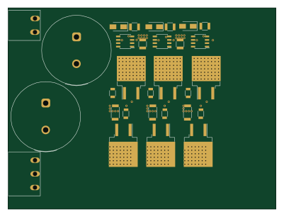
Trollerv2
100 × 75 mm33 parts4LGPL-3.0979