
S6la8

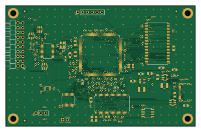
About the S6la8 PCB
S6la8 is an open source PCB design by OutBlade, published on GitHub. It is a 4-layer board measuring 100 × 64 mm, with 148 components from 42 distinct parts.
Other key parts include the 24LC128-I/SN, USBLC6-2SC6, SN74LVC245APWR, SN74LVC8T245PWR and SN74LVC2T45DCUR. By type, the board carries 61 resistors, 58 capacitors, 14 ICs, 5 connectors, 4 diodes and 4 inductors.
It belongs with the test & measurement designs in this gallery.
From the project
Open-source 8-channel logic analyzer: FX2LP + Spartan-6, with a sigrok driver. Design in progress, not yet built or tested.
An open-source 8-channel logic analyzer built around a Cypress/Infineon CY7C68013A (FX2LP) USB controller and a Xilinx Spartan-6 XC6SLX9 FPGA, with a driver for sigrok.
No board has been manufactured. No FPGA bitstream has been built. Nothing in this repository has run on real hardware. Do not order this board yet.
The schematic is in docs/schematic.pdf. It is one very large generated sheet and still needs to be split into readable pages.
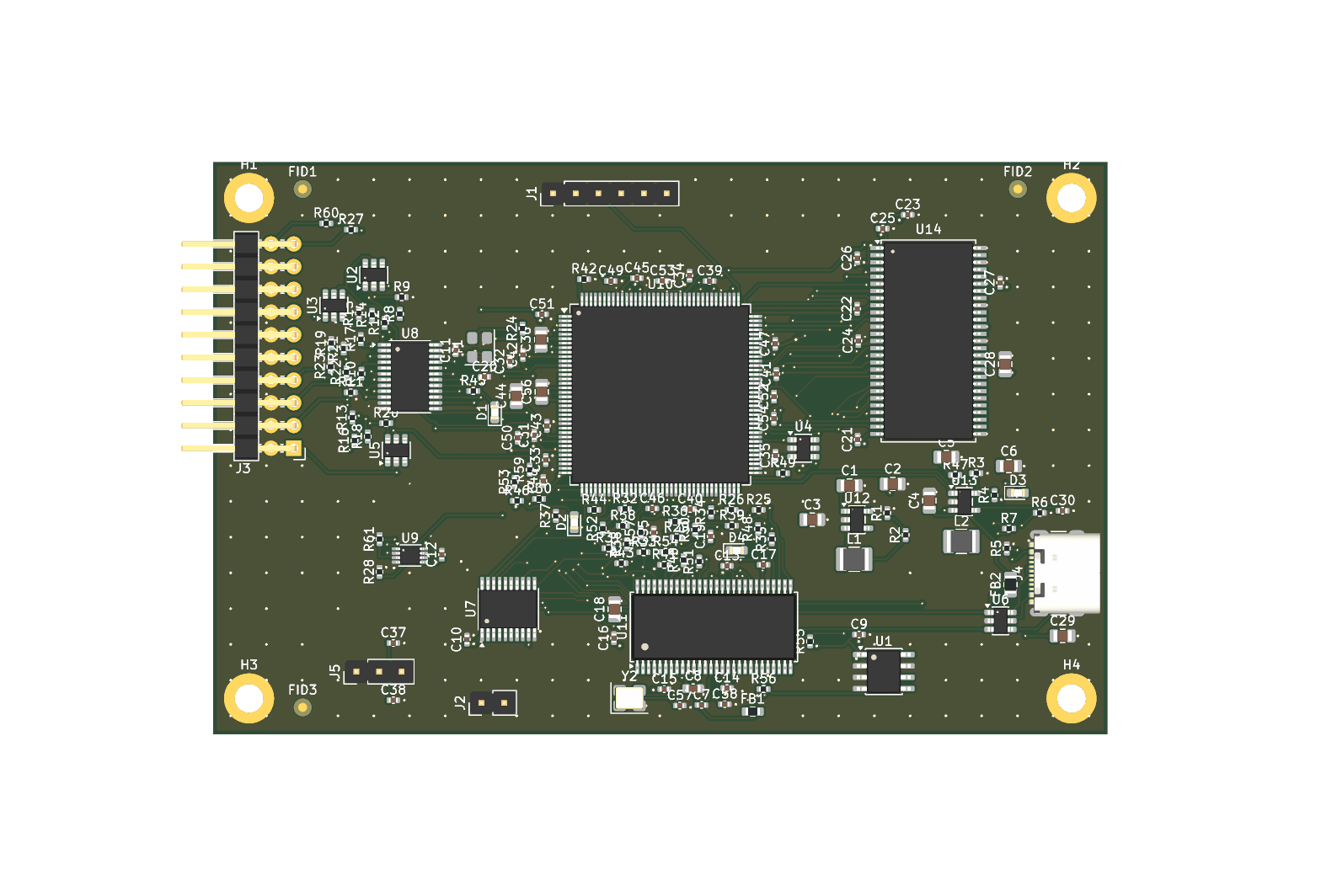
Main components on the S6la8
S6la8 bill of materials (BOM)
148 components, 42 distinct parts.
| Qty | Part | Footprint | Refs |
|---|---|---|---|
| 1 | 24LC128-I/SN Microchip | SOIC-8_3.9x4.9mm_P1.27mm | U1 |
| 5 | USBLC6-2SC6 STMicroelectronics | SOT-23-6 | U2, U3, U4, U5, U6 |
| 1 | SN74LVC245APWR Texas Instruments | TSSOP-20_4.4x6.5mm_P0.65mm | U7 |
| 1 | SN74LVC8T245PWR Texas Instruments | TSSOP-24_4.4x7.8mm_P0.65mm | U8 |
| 1 | SN74LVC2T45DCUR Texas Instruments | VSSOP-8_2.3x2mm_P0.5mm | U9 |
| 1 | XC6SLX9-2TQG144C AMD | TQFP-144_20x20mm_P0.5mm | U10 |
| 1 | CY7C68013A-56PVXC Infineon | SSOP-56_7.5x18.5mm_P0.635mm | U11 |
| 2 | TLV62569DBVR Texas Instruments | SOT-23-5 | U12, U13 |
| 1 | MT48LC16M16A2P-6A Micron | TSOP-II-54_22.2x10.16mm_P0.8mm | U14 |
| 1 | ASE-50.000MHZ-LC-T Abracon | Oscillator_SMD_Abracon_ASE-4Pin_3.2x2.5mm | Y1 |
| 1 | 24MHz 12pF | Crystal_SMD_3225-4Pin_3.2x2.5mm | Y2 |
| 1 | 2.54mm 6 x 1 THT Vertical Male | PinHeader_1x06_P2.54mm_Vertical | J1 |
| 1 | 2.54mm 2 x 1 THT Vertical Male | PinHeader_1x02_P2.54mm_Vertical | J2 |
| 1 | 2.54mm 10 x 2 THT Horizontal Male | PinHeader_2x10_P2.54mm_Horizontal | J3 |
| 1 | USB4105-GF-A GCT | USB_C_Receptacle_GCT_USB4105-xx-A_16P_TopMnt_Horizontal | J4 |
| 1 | 2.54mm 3 x 1 THT Vertical Male | PinHeader_1x03_P2.54mm_Vertical | J5 |
| 2 | LED GREEN | LED_0603_1608Metric | D1, D3 |
| 1 | LED RED | LED_0603_1608Metric | D2 |
| 1 | LED YELLOW | LED_0603_1608Metric | D4 |
| 1 | 220 100MHz | R_0603_1608Metric | FB1 |
Show 22 more
| Qty | Part | Footprint | Refs |
|---|---|---|---|
| 1 | 220 100MHz | R_0805_2012Metric | FB2 |
| 2 | DFE322512F-2R2M=P2 2.2uH Murata | L_1210_3225Metric | L1, L2 |
| 3 | 10uF 10V | C_0805_2012Metric | C1, C4, C29 |
| 4 | 22uF 6.3V | C_0805_2012Metric | C2, C3, C5, C6 |
| 39 | 100nF 6.3V | C_0402_1005Metric | C7, C9, C10, C11, C12, C13, C14, C15 +31 |
| 1 | 2.2uF 6.3V | C_0603_1608Metric | C8 |
| 3 | 4.7uF 6.3V | C_0805_2012Metric | C18, C36, C44 |
| 1 | 1uF | C_0402_1005Metric | C19 |
| 2 | 10uF 6.3V | C_0805_2012Metric | C28, C56 |
| 2 | 100nF 10V | C_0402_1005Metric | C30, C37 |
| 1 | 1uF 10V | C_0402_1005Metric | C38 |
| 2 | 18pF | C_0402_1005Metric | C57, C58 |
| 14 | 100k | R_0402_1005Metric | R1, R2, R3, R9, R11, R13, R15, R17 +6 |
| 1 | 453k | R_0402_1005Metric | R4 |
| 2 | 5.1k | R_0402_1005Metric | R5, R6 |
| 11 | 33 | R_0402_1005Metric | R7, R24, R29, R30, R31, R32, R33, R34 +3 |
| 10 | 100 | R_0402_1005Metric | R8, R10, R12, R14, R16, R18, R20, R22 +2 |
| 7 | 1k | R_0402_1005Metric | R25, R42, R45, R46, R47, R48, R54 |
| 1 | 330 | R_0402_1005Metric | R26 |
| 9 | 10k | R_0402_1005Metric | R37, R38, R39, R41, R51, R52, R57, R58 +1 |
| 4 | 4.7k | R_0402_1005Metric | R44, R49, R50, R53 |
| 2 | 2.2k | R_0402_1005Metric | R55, R56 |
S6la8 design files
The KiCad project lives in the OutBlade/s6la8 repository on GitHub; these links point at the commit this page was built from.
- Layouthardware/eda/s6la8.kicad_pcb
- Schematichardware/eda/s6la8.kicad_sch
S6la8: common questions
How big is the S6la8 PCB?
The S6la8 measures 100 × 64 mm, has 4 copper layers and is 1.6062 mm thick.
How many components are on the S6la8?
148 components, from 42 distinct parts. The full bill of materials is listed on this page.
Where can I download the S6la8 design files?
From the OutBlade/s6la8 repository on GitHub, which has the KiCad layout and the schematic; the links under Design files point to each one.
Can I use the S6la8 design in my own project?
The repository has no license, so all rights stay with OutBlade. Use it as a reference, and ask the author before reusing the design.
Similar boards
AnalyzerBoxPCB fork
gusmanb
52.7 × 47.9 mm54 parts4LGPL-3.05.0k
LevelShifter
28.3 × 39.8 mm21 parts2LGPL-3.05.0k
StackLink
52.3 × 10.5 mm5 parts2LGPL-3.05.0k
EleLab v2 Frontpanel a
Chrismettal
88 × 25 mm23 parts2LGPL-3.0528
EleLab v2 Bus150
150 × 50 mm37 parts2LGPL-3.0528
EleLab v2 PowerFeed
68 × 50 mm11 parts2LGPL-3.0528