
EDA-AI-Sensor-Interface-Lab


About the EDA-AI-Sensor-Interface-Lab PCB
EDA-AI-Sensor-Interface-Lab is an open source PCB design by rodriguez46p-ui, published on GitHub under the MIT license. It is a 2-layer board measuring 70 × 38 mm, with 5 components from 5 distinct parts.
Other key parts include the INA333AIDGKR, OPA333AIDBVR and MCP1700T-3302E/TT. By type, the board carries 3 ICs and 2 connectors.
It belongs with the sensors designs in this gallery.
From the project
Low-noise sensor front-end EDA portfolio with KiCad assets, SPICE simulations, BOM, reports, and QA automation
Low-noise sensor front-end and power conditioning board for AI research data acquisition. This is a runnable portfolio project for an Electronics Design & Simulation (EDA) Specialist role: it generates KiCad-facing design files, Ngspice-compatible simulation decks, numerical fallback simulation outputs, BOMs, plots, QA checks, and review reports.
The project shows schematic thinking, SPICE simulation, open EDA workflow design, manufacturability notes, digital asset QA, and reproducible automation. It is intentionally built without paid tools or private vendor models so a reviewer can clone…
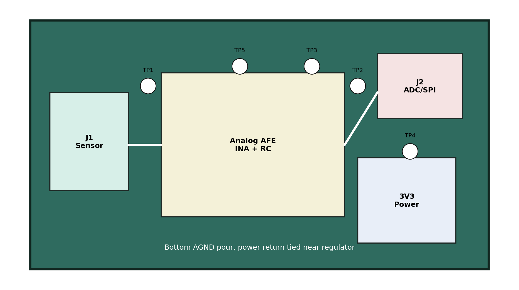
Main components on the EDA-AI-Sensor-Interface-Lab
EDA-AI-Sensor-Interface-Lab bill of materials (BOM)
5 components, 5 distinct parts — part numbers from the project's BOM.
| Qty | Part | Footprint | Refs |
|---|---|---|---|
| 1 | INA333AIDGKR INA333-class Texas Instruments | VSSOP-8_3x3mm_P0.65mm | U1 |
| 1 | OPA333AIDBVR OPA333-class Texas Instruments | SOT-23-5 | U2 |
| 1 | MCP1700T-3302E/TT MCP1700-3302 Microchip | SOT-23 | U3 |
| 1 | S4B-PH-SM4-TB Sensor input JST | JST_PH_S4B-PH-SM4-TB | J1 |
| 1 | TSW-106-07-G-S ADC/SPI header Samtec | PinHeader_1x06_P2.54mm_Vertical | J2 |
EDA-AI-Sensor-Interface-Lab design files
The KiCad project lives in the rodriguez46p-ui/EDA-AI-Sensor-Interface-Lab repository on GitHub; these links point at the commit this page was built from.
EDA-AI-Sensor-Interface-Lab: common questions
How big is the EDA-AI-Sensor-Interface-Lab PCB?
The EDA-AI-Sensor-Interface-Lab measures 70 × 38 mm, has 2 copper layers and is 1.6 mm thick.
How many components are on the EDA-AI-Sensor-Interface-Lab?
5 components, from 5 distinct parts, with part numbers taken from the project's own BOM. The full bill of materials is listed on this page.
Where can I download the EDA-AI-Sensor-Interface-Lab design files?
From the rodriguez46p-ui/EDA-AI-Sensor-Interface-Lab repository on GitHub, which has the KiCad layout, the schematic and the BOM; the links under Design files point to each one.
Can I use the EDA-AI-Sensor-Interface-Lab design in my own project?
Yes, under the terms of its MIT license, which rodriguez46p-ui chose for the repository.
Similar boards
Sensor smd
scottbez1
40 × 20 mm5 parts2LApache-2.04.2k
Sensors
StuckAtPrototype
15.2 × 9 mm14 parts4LApache-2.03.8k
Microphone
Mentra-Community
5.5 × 6.1 mm6 parts2LMIT1.2k
TemperaturePCB PANEL
stuartpittaway
116 × 75.5 mm178 parts2LCC-BY-NC-4.01.1k
Pots
shanteacontrols
390 × 93 mm75 parts2LApache-2.0956
ButtonsLEDs
390 × 37 mm82 parts2LApache-2.0956