
Pcb dev fpga iCE40

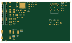
About the Pcb dev fpga iCE40
Pcb dev fpga iCE40 is an open source FPGA PCB design by shishir-dey, published on GitHub under the MIT license. It is a 2-layer board measuring 75.3 × 43.3 mm, with 50 components from 26 distinct parts.
Its main chip is the ICE40UP5K-SG48ITR, from the FPGA family. Other key parts include the LY68L6400, W25Q128JVxxM, TLV75533PDRV, TLV73312PDBV and USBLC6-2P6. By type, the board carries 19 capacitors, 16 resistors, 6 ICs, 4 diodes, 3 connectors and 1 crystal.
It belongs with the dev boards & breakouts designs in this gallery.
From the project
A 2 layer development board with a Lattice Semiconductor ICE40UP5K-SG48ITR FPGA. Made with KiCad
Main components on the Pcb dev fpga iCE40
Pcb dev fpga iCE40 bill of materials (BOM)
50 components, 26 distinct parts.
| Qty | Part | Footprint | Refs |
|---|---|---|---|
| 1 | ICE40UP5K-SG48ITR | QFN-48-1EP_7x7mm_P0.5mm_EP5.6x5.6mm | U1 |
| 1 | LY68L6400 | SOIC127P600X175-8N | U2 |
| 1 | W25Q128JVxxM | SOIC127P1032X264-16N | U3 |
| 1 | TLV75533PDRV | WSON-6-1EP_2x2mm_P0.65mm_EP1x1.6mm | U4 |
| 1 | TLV73312PDBV | SOT-23-5 | U5 |
| 1 | USBLC6-2P6 | SOT-666 | U6 |
| 1 | 12MHz | Crystal_SMD_0603-4Pin_6.0x3.5mm | Y1 |
| 1 | Header 1 | PinHeader_1x10_P2.54mm_Vertical | J1 |
| 1 | Header 2 | PinHeader_1x10_P2.54mm_Vertical | J2 |
| 1 | USB-C Receptacle (USB2.0) | 632723300021 | J3 |
| 1 | SPST Switch | SW_SPST_B3S-1000 | SW1 |
| 1 | RED_LED | LED_0603_1608Metric | D1 |
| 1 | GREEN_LED | LED_0603_1608Metric | D2 |
| 1 | BLUE_LED | LED_0603_1608Metric | D3 |
| 1 | RGB LED | LED_RGB_1210 | D4 |
| 9 | 100n | C_0603_1608Metric | C1, C2, C3, C4, C6, C7, C11, C12 +1 |
| 3 | 1u | C_0603_1608Metric | C5, C9, C15 |
| 2 | 10n | C_0603_1608Metric | C8, C13 |
| 1 | 10u | C_0603_1608Metric | C10 |
| 4 | 4u7 | C_0603_1608Metric | C16, C17, C18, C19 |
Show 6 more
| Qty | Part | Footprint | Refs |
|---|---|---|---|
| 3 | 2k2 | R_0603_1608Metric | R1, R2, R3 |
| 7 | 10k | R_0603_1608Metric | R4, R5, R6, R8, R9, R10, R11 |
| 1 | 100e | R_0603_1608Metric | R7 |
| 2 | 5k1 | R_0603_1608Metric | R12, R13 |
| 1 | 1k5 | R_0603_1608Metric | R14 |
| 2 | 22e | R_0603_1608Metric | R15, R16 |
Pcb dev fpga iCE40 design files
The KiCad project lives in the shishir-dey/pcb-dev-fpga-iCE40 repository on GitHub; these links point at the commit this page was built from.
Pcb dev fpga iCE40: common questions
What microcontroller does the Pcb dev fpga iCE40 use?
The Pcb dev fpga iCE40 is built around the ICE40UP5K-SG48ITR, from the FPGA family.
How big is the Pcb dev fpga iCE40?
The Pcb dev fpga iCE40 measures 75.3 × 43.3 mm, has 2 copper layers and is 1.6 mm thick.
How many components are on the Pcb dev fpga iCE40?
50 components, from 26 distinct parts. The full bill of materials is listed on this page.
Where can I download the Pcb dev fpga iCE40 design files?
From the shishir-dey/pcb-dev-fpga-iCE40 repository on GitHub, which has the KiCad layout and the schematic; the links under Design files point to each one.
Can I use the Pcb dev fpga iCE40 design in my own project?
Yes, under the terms of its MIT license, which shishir-dey chose for the repository.
Can I test firmware for the Pcb dev fpga iCE40 without the hardware?
Yes. HardLabs builds a simulation of the board from its netlist and BOM, so you can run and debug FPGA firmware against it before you order a PCB.
Similar boards
 FPGA
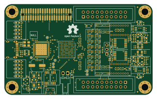
FPGABase board
GlasgowEmbedded
80 × 49 mm222 parts4L0BSD2.2k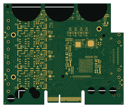 FPGA
FPGAThunderscope Rev5.3
EEVengers
122.5 × 103.5 mm817 parts6LMIT1.3k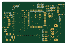 FPGA
FPGAUsb sniffer
ataradov
58.2 × 38.1 mm86 parts2LBSD-3-Clause1.3k FPGA
FPGATomu, I'm
theacodes
13 × 9.4 mm40 parts4LMIT1.1k FPGA
FPGAIcepi zero
cheyao
65 × 30 mm143 parts4LSHL-2.1828 FPGA
FPGAGcvideo
ikorb
49 × 30 mm44 parts4LNo license765