
Backplane

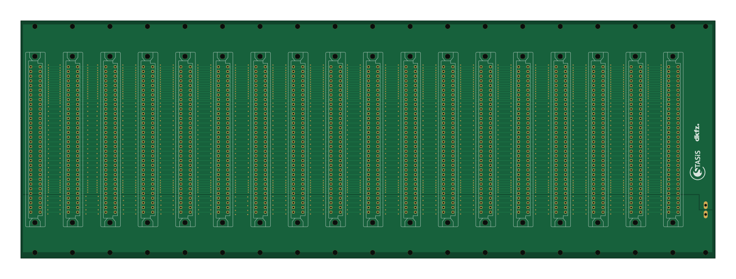
About the Backplane PCB
Backplane is an open source PCB design by sOrzada, published on GitHub under the CERN-OHL-W-2.0 license. It is a 2-layer board measuring 376 × 128.6 mm, with 75 components from 4 distinct parts.
By type, the board carries 19 crystals and 18 capacitors.
From the project
This is the repository for the exposition hardware of the STASIS project.
This Folder contains the PCBs and Housings for the Control System of the STASIS project's RF exposition system. The PCBs are provided in two different formats: Eagle and KiCAD. The Housings-folder contains .step files for the housings and front panels of the Eurocards.
Backplane bill of materials (BOM)
75 components, 4 distinct parts.
| Qty | Part | Footprint | Refs |
|---|---|---|---|
| 18 | FAC64S | FAC64S_194 | X1, X2, X3, X4, X5, X6, X7, X8 +10 |
| 1 | AKL320-2 | MSTBV2_175 | X19 |
| 38 | — | @HOLE0, @HOLE1, @HOLE2, @HOLE3, @HOLE4, @HOLE5, @HOLE6, @HOLE7 +30 | |
| 18 | 10nF | C0603_334 | C1, C2, C3, C4, C5, C6, C7, C8 +10 |
Backplane design files
The KiCad project lives in the sOrzada/STASIS_Exposure_Hardware repository on GitHub; these links point at the commit this page was built from.
Backplane: common questions
How big is the Backplane PCB?
The Backplane measures 376 × 128.6 mm, has 2 copper layers and is 1.6 mm thick.
How many components are on the Backplane?
75 components, from 4 distinct parts. The full bill of materials is listed on this page.
Where can I download the Backplane design files?
From the sOrzada/STASIS_Exposure_Hardware repository on GitHub, which has the KiCad layout and the schematic; the links under Design files point to each one.
Can I use the Backplane design in my own project?
Yes, under the terms of its CERN-OHL-W-2.0 license, which sOrzada chose for the repository.
More boards in STASIS_Exposure_Hardware
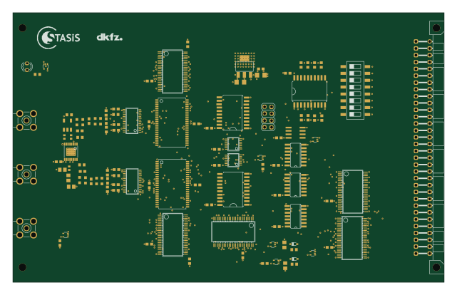
Modulator V1p2
160 × 100 mm112 parts6LCERN-OHL-W-2.00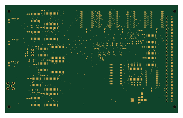
Timing Control V1p1
160 × 100 mm101 parts6LCERN-OHL-W-2.00
Stripline
450 × 100 mm81 parts2LCERN-OHL-W-2.00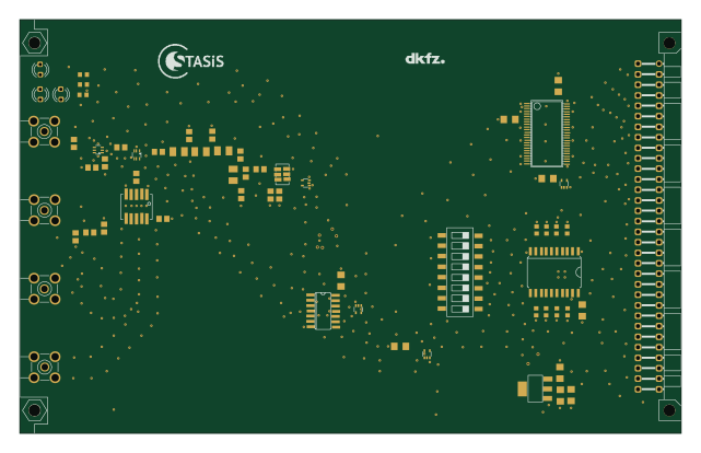
Signal source V1p0
160 × 100 mm63 parts2LCERN-OHL-W-2.00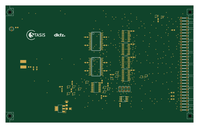
SPI2Parallel v1p1
160 × 100 mm63 parts4LCERN-OHL-W-2.00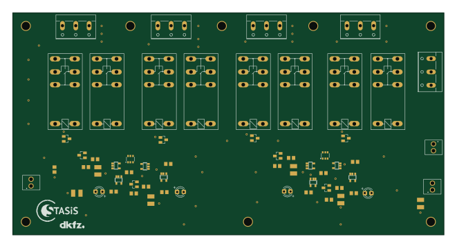
Power Distribution V1.1
165 × 85 mm61 parts2LCERN-OHL-W-2.00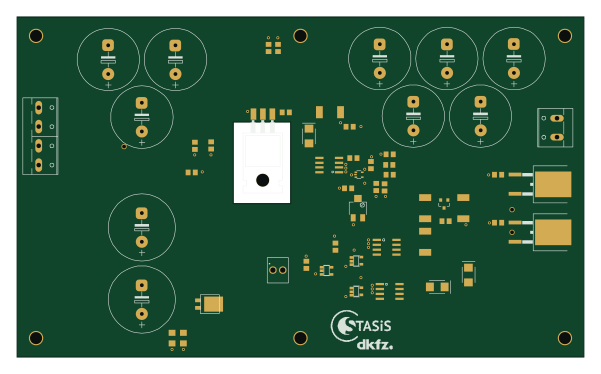
VoltageControl V1p1
150 × 90 mm55 parts2LCERN-OHL-W-2.00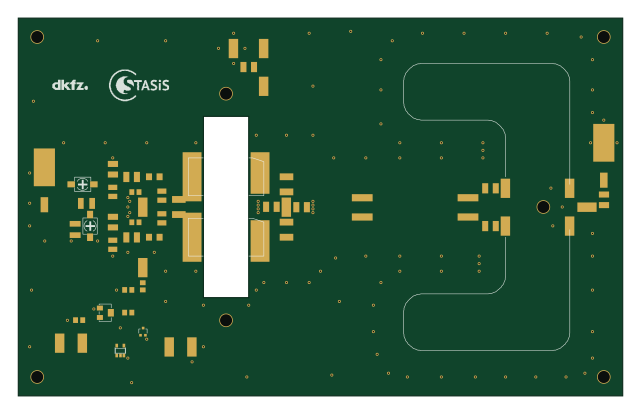
HPA Module V1p1
160 × 100 mm52 parts2LCERN-OHL-W-2.00
RF Splitter active
160 × 100 mm19 parts2LCERN-OHL-W-2.00
USB2SPI
160 × 100 mm12 parts2LCERN-OHL-W-2.00
TR UBL Splitter V1p1
160 × 100 mm9 parts2LCERN-OHL-W-2.00