
Split flap

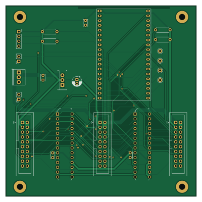
About the Split flap PCB
Split flap is an open source ESP32 PCB design by tinkermax, published on GitHub under the CC-BY-4.0 license. It is a 2-layer board measuring 99.9 × 99.9 mm, with 24 components from 14 distinct parts.
Its main chip is the ESP32-DevKitC, from the ESP32 family. Other key parts include the LD1117V33 and MCP23017-E/SP. By type, the board carries 7 connectors, 5 capacitors, 4 ICs, 4 test points and 4 resistors.
It belongs with the displays & leds designs in this gallery.
From the project
DIY mechanical spli-flap display
This is an alternate electronics and firmware for David Kingsman's Split-Flap Display.
MYNTPSERVER "au.pool.ntp.org" // Set the best fitting NTP server (pool) for your location MYTZ "AEST-10AEDT,M10.1.0,M4.1.0/3" // Set your time zone from https://github.com/nayarsystems/posixtz_db/blob/master/zones.csv
WORDNIKAPIKEY "" // Get your private key from https://developer.wordnik.com/ MINWORDLEN 9 // Specify minimum word length to fetch from Wordnik WORDUPDATESPERHOUR 1 // Set number of word updates from https://wordnik.com per hour. 0 will disable, else use an integer that results in an exact…

Main components on the Split flap
Split flap bill of materials (BOM)
24 components, 14 distinct parts — part numbers from the project's BOM.
| Qty | Part | Footprint | Refs |
|---|---|---|---|
| 1 | LD1117V33 STMicroelectronics | TO-220-3 | U1 |
| 1 | ESP32-DevKitC | ESP32-DevKitC | U2 |
| 2 | MCP23017-E/SP MCP23017 Microchip Technology | DIP-28_W7.62mm | U3, U4 |
| 1 | +9V IN | TerminalBlock_TE_282834-3_1x03_P2.54mm_Horizontal | J1 |
| 1 | Chain I2C | PinSocket_1x04_P2.54mm_Vertical | J2 |
| 1 | SENS3 Button1 | PinSocket_1x02_P2.54mm_Vertical | J3 |
| 1 | Button2 | PinSocket_1x02_P2.54mm_Vertical | J4 |
| 1 | SENS2 Units 0-3 | IDC-Header_2x10_P2.54mm_Vertical | J5 |
| 1 | Units 4-7 | IDC-Header_2x10_P2.54mm_Vertical | J6 |
| 1 | SENS1 Units 8-11 | IDC-Header_2x10_P2.54mm_Vertical | J7 |
| 4 | 5000 Keystone Electronics | Test_Point_D1.02mm | TP1, TP2, TP3, TP4 |
| 4 | 100UF 100nF | C_Disc_D3.4mm_W2.1mm_P2.50mm | C1, C3, C4, C5 |
| 1 | 100UF 10uF | CP_Radial_D5.0mm_P2.00mm | C2 |
| 4 | 4K7 | R_Axial_DIN0207_L6.3mm_D2.5mm_P7.62mm_Horizontal | R1, R2, R3, R4 |
Split flap design files
The KiCad project lives in the tinkermax/split-flap repository on GitHub; these links point at the commit this page was built from.
Split flap: common questions
What microcontroller does the Split flap use?
The Split flap is built around the ESP32-DevKitC, from the ESP32 family.
How big is the Split flap PCB?
The Split flap measures 99.9 × 99.9 mm, has 2 copper layers and is 1.6 mm thick.
How many components are on the Split flap?
24 components, from 14 distinct parts, with part numbers taken from the project's own BOM. The full bill of materials is listed on this page.
Where can I download the Split flap design files?
From the tinkermax/split-flap repository on GitHub, which has the KiCad layout, the schematic and the BOM; the links under Design files point to each one.
Can I use the Split flap design in my own project?
Yes, under the terms of its CC-BY-4.0 license, which tinkermax chose for the repository.
Can I test firmware for the Split flap without the hardware?
Yes. HardLabs builds a simulation of the board from its netlist and BOM, so you can run and debug ESP32 firmware against it before you order a PCB.
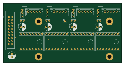
More boards in split-flap
Similar boards
 ESP32
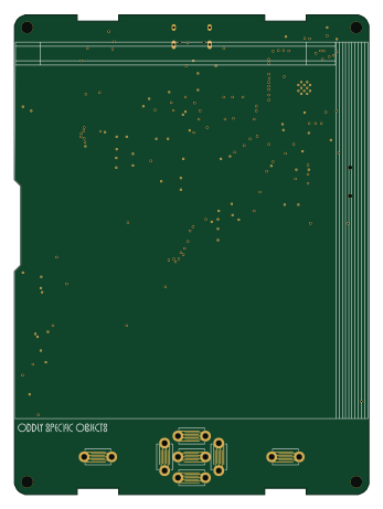
ESP32Open Book Abridged Edition
joeycastillo
85 × 115 mm65 parts2LCC-BY-SA-4.08.1k ESP32
ESP32Esp32 minimal
atopile
36.2 × 26.8 mm20 parts2LMIT4.0k ESP32
ESP32Badge
56.3 × 39 mm239 parts4LMIT4.0k ESP32
ESP32Controller
StuckAtPrototype
29 × 74 mm58 parts4LApache-2.03.8k ESP32
ESP32Racer
36 × 50.2 mm70 parts4LApache-2.03.8k ESP32
ESP32Bitaxe
skot
56.5 × 99.8 mm86 parts4LCERN-OHL-S-2.01.4k