
Sensor testing

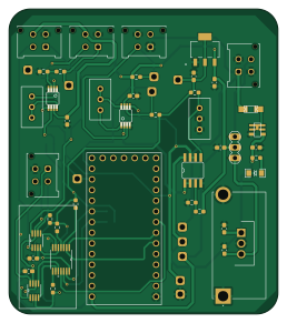
About the Sensor testing PCB
Sensor testing is an open source PCB design by Vedika-Doke, published on GitHub. It is a 2-layer board measuring 63.9 × 72.6 mm, with 61 components from 28 distinct parts.
Other key parts include the L7805CV-DG, HSS10-B20-P40, DEV-15583, TXS0102DCTR and TCA9543APWR. By type, the board carries 18 resistors, 9 switches, 8 ICs, 7 test points, 5 connectors and 1 fuse.
It belongs with the sensors designs in this gallery.
From the project
This repository contains my academic projects, research work, and hands-on engineering experience across core electrical engineering, embedded systems, digital design, and hardware development.
Main components on the Sensor testing
Sensor testing bill of materials (BOM)
61 components, 28 distinct parts.
| Qty | Part | Footprint | Refs |
|---|---|---|---|
| 1 | L7805CV-DG | TO255P460X1020X2008-3P | IC1 |
| 1 | HSS10-B20-P40 | HSS10B20P40 | U1 |
| 1 | DEV-15583 | MODULE_DEV-15583 | U2 |
| 2 | TXS0102DCTR | DCT8 | U3, U5 |
| 1 | TCA9543APWR | PW14 | U4 |
| 1 | ZLDO1117G33TA | SOT_G33TA_DIO | U6 |
| 1 | TSOP-6_PMOS | TSOP-6_PMOS | U$2 |
| 5 | 430450412 | Molex_Micro-Fit_3.0_43045-0412_2x02_P3.00mm_Vertical | J1, J2, J3, J4, J5 |
| 2 | TPSQPAD1-13 | P1-13_385 | +3V3, ST_FR+2 |
| 2 | INA333 | MSOP8 | DA1, DA2 |
| 1 | ~ | SO8 | DOA1 |
| 1 | 1206L | 1206L | F1 |
| 1 | 0.33uF | C_0603_1608Metric_Pad1.08x0.95mm_HandSolder | IN_CAP1 |
| 1 | 0.1uF | C_0603_1608Metric_Pad1.08x0.95mm_HandSolder | OUT_CAP1 |
| 6 | 0.1uF | C_0603_1608Metric_Pad1.08x0.95mm_HandSolder | S-1, S-2, S-6, S-7, S-8, S-9 |
| 1 | 0.33uF | C_0603_1608Metric_Pad1.08x0.95mm_HandSolder | S-3 |
| 1 | 1uF | C_0603_1608Metric_Pad1.08x0.95mm_HandSolder | S-4 |
| 1 | 1nF | C_0603_1608Metric_Pad1.08x0.95mm_HandSolder | S-5 |
| 1 | MA03-1 | MA03-1_162 | SV4 |
| 7 | TPSQPAD1-13 | P1-13_385 | TP1, TP2, TP3, TP5, TP7, TP9, TP10 |
Show 8 more
| Qty | Part | Footprint | Refs |
|---|---|---|---|
| 2 | 3296W-1-101LF | Potentiometer_Bourns_3296W_Vertical | VR1, VR2 |
| 1 | 10k | Potentiometer_Bourns_3296W_Vertical | VR3 |
| 1 | LED1206 | LED-1206 | UNK12V_LED1 |
| 1 | 10uF | C_0603_1608Metric_Pad1.08x0.95mm_HandSolder | C1 |
| 2 | 7k | R_0603_1608Metric_Pad0.98x0.95mm_HandSolder | R1, R4 |
| 2 | 5k | R_0603_1608Metric_Pad0.98x0.95mm_HandSolder | R2, R5 |
| 13 | 10k | R_0603_1608Metric_Pad0.98x0.95mm_HandSolder | R3, R6, R7, R8, R11, R12, R13, R15 +5 |
| 1 | 120 | R_0603_1608Metric_Pad0.98x0.95mm_HandSolder | R10 |
Sensor testing design files
The KiCad project lives in the Vedika-Doke/EE_Wisdom repository on GitHub; these links point at the commit this page was built from.
Sensor testing: common questions
How big is the Sensor testing PCB?
The Sensor testing measures 63.9 × 72.6 mm, has 2 copper layers and is 1.6 mm thick.
How many components are on the Sensor testing?
61 components, from 28 distinct parts. The full bill of materials is listed on this page.
Where can I download the Sensor testing design files?
From the Vedika-Doke/EE_Wisdom repository on GitHub, which has the KiCad layout and the schematic; the links under Design files point to each one.
Can I use the Sensor testing design in my own project?
The repository has no license, so all rights stay with Vedika-Doke. Use it as a reference, and ask the author before reusing the design.
More boards in EE_Wisdom
Similar boards
Sensor smd
scottbez1
40 × 20 mm5 parts2LApache-2.04.2k
Sensors
StuckAtPrototype
15.2 × 9 mm14 parts4LApache-2.03.8k
Microphone
Mentra-Community
5.5 × 6.1 mm6 parts2LMIT1.2k
TemperaturePCB PANEL
stuartpittaway
116 × 75.5 mm178 parts2LCC-BY-NC-4.01.1k
Pots
shanteacontrols
390 × 93 mm75 parts2LApache-2.0956
USB
52 × 12.6 mm6 parts2LApache-2.0956