
Delay reverb

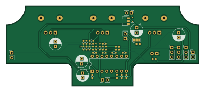
About the Delay reverb PCB
Delay reverb is an open source PCB design by adeboni, published on GitHub. It is a 2-layer board measuring 100 × 42 mm, with 46 components from 26 distinct parts.
Other key parts include the PT2399 and L78L05_SOT89. By type, the board carries 17 capacitors, 13 resistors, 5 connectors, 3 switches, 2 ICs and 2 diodes.
It belongs with the audio, iot & wireless and sensors designs in this gallery.
From the project
This repository stores code for various electronics projects I've made
This repository stores code for various electronics projects I've made
Wasp Cannon: A wifi-enabled water cannon for shooting water at wasps on my balcony CV Glove: A glove with flex sensors on fingers that output control voltages for eurorack modules Critter Coat: A coat with fluttering butterflies on it AQI Monitor: Simple air quality monitor using a Honeywell HPM sensors Atari Controller: Custom Atari 2600 controller with an analog joystick Camera Remote: Wireless camera shutter control Gas Sensor: A generic MQ gas sensor board with LED indicators PS2 Drone Controller: Lets you control…
Main components on the Delay reverb
Delay reverb bill of materials (BOM)
46 components, 26 distinct parts — part numbers from the project's BOM.
| Qty | Part | Footprint | Refs |
|---|---|---|---|
| 1 | PT2399 | DIP-16_W7.62mm | U1 |
| 1 | L78L05_SOT89 | SOT-89-3 | U7 |
| 5 | Conn_01x02 | PinHeader_1x02_P2.54mm_Vertical | J2, J3, J4, J5, J6 |
| 1 | SolderJumper_3_Bridged12 | SolderJumper-3_P1.3mm_Bridged12_Pad1.0x1.5mm | JP1 |
| 2 | B50k | Potentiometer_Alpha_RD901F-40-00D_Single_Vertical | RV1, RV2 |
| 1 | B20k | Potentiometer_Alpha_RD901F-40-00D_Single_Vertical | RV3 |
| 3 | SW_SPDT | PinHeader_1x03_P2.54mm_Vertical | SW1, SW2, SW3 |
| 1 | 1N5819WS | D_SOD-323 | D1 |
| 1 | LED | LED_D5.0mm | D2 |
| 2 | 4.7U 4.7u | C_0603_1608Metric | C1, C3 |
| 2 | 10u | CP_Radial_D6.3mm_P2.50mm | C2, C5 |
| 1 | 3.9N 3.9n | C_0603_1608Metric | C4 |
| 1 | 10N 10n | C_0603_1608Metric | C6 |
| 1 | 3.3N 3.3n | C_0603_1608Metric | C7 |
| 3 | 47u | CP_Radial_D6.3mm_P2.50mm | C14, C40, C41 |
| 2 | 82N 82n | C_0603_1608Metric | C45, C46 |
| 2 | 560P 560p | C_0603_1608Metric | C47, C48 |
| 3 | 100N 100n | C_0603_1608Metric | C49, C50, C51 |
| 4 | 10K 10k | R_0603_1608Metric | R1, R2, R6, R7 |
| 2 | 15K 15k | R_0603_1608Metric | R3, R9 |
Show 6 more
| Qty | Part | Footprint | Refs |
|---|---|---|---|
| 1 | 5.6K 5.6k | R_0603_1608Metric | R4 |
| 1 | 4.7K 4.7k | R_0603_1608Metric | R5 |
| 1 | 18K 18k | R_0603_1608Metric | R8 |
| 1 | 100K 100k | R_0603_1608Metric | R10 |
| 2 | 1k | R_0603_1608Metric | R11, R35 |
| 1 | 200K 200k | R_0603_1608Metric | R12 |
Delay reverb design files
The KiCad project lives in the adeboni/electronics repository on GitHub; these links point at the commit this page was built from.
Delay reverb: common questions
How big is the Delay reverb PCB?
The Delay reverb measures 100 × 42 mm, has 2 copper layers and is 1.6 mm thick.
How many components are on the Delay reverb?
46 components, from 26 distinct parts, with part numbers taken from the project's own BOM. The full bill of materials is listed on this page.
Where can I download the Delay reverb design files?
From the adeboni/electronics repository on GitHub, which has the KiCad layout, the schematic and the BOM; the links under Design files point to each one.
Can I use the Delay reverb design in my own project?
The repository has no license, so all rights stay with adeboni. Use it as a reference, and ask the author before reusing the design.
More boards in electronics
 RP2040/RP2350
Ir receiver
100 × 100 mm84 parts2LNo license0 RP2040/RP2350
Ir transmitter
114.3 × 25.4 mm81 parts2LNo license0
Looper
100 × 62 mm63 parts2LNo license0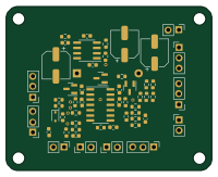
Alien screamer
50 × 40 mm55 parts2LNo license0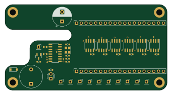
Drone tranceiver
85 × 45 mm40 parts2LNo license0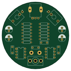
Tape jar
58 × 58 mm28 parts2LNo license0
Aw rachio adapter
23.1 × 51 mm19 parts2LNo license0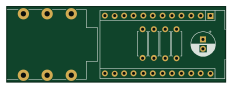 AVR/Arduino
Drum trigger adapter
58 × 20 mm7 parts2LNo license0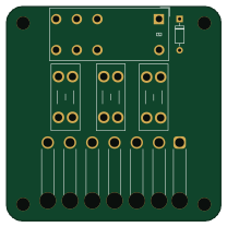
Fiat light relay
52 × 52 mm7 parts2LNo license0
Dc dc jack converter
30.8 × 12.2 mm5 parts2LNo license0
Tape jar fp
68 × 68 mm3 parts2LNo license0
Similar boards
Sensor smd
scottbez1
40 × 20 mm5 parts2LApache-2.04.2k
Sensors
StuckAtPrototype
15.2 × 9 mm14 parts4LApache-2.03.8k
EinkPDA screen
TalismanDesign
95 × 54 mm27 parts2LApache-2.02.0k
Microphone
Mentra-Community
5.5 × 6.1 mm6 parts2LMIT1.2k
KLOR
GEIGEIGEIST
160.2 × 118.3 mm79 parts2LGPL-3.01.2k
TemperaturePCB PANEL
stuartpittaway
116 × 75.5 mm178 parts2LCC-BY-NC-4.01.1k