
Hangbot breakout

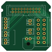
About the Hangbot breakout
Hangbot breakout is an open source PCB design by ep-infosec, published on GitHub under the CC-BY-4.0 license. It is a 2-layer board measuring 42 × 42 mm, with 8 components from 5 distinct parts.
It belongs with the dev boards & breakouts designs in this gallery.
From the project
This repository houses various things (3D models, circuits, class materials) that we've created for use in Google makerspaces.
This repository houses various things (3D models, circuits, class materials) that we've created for use in Google makerspaces.
If you'd like to contribute, see CONTRIBUTING
Hangbot breakout bill of materials (BOM)
8 components, 5 distinct parts.
| Qty | Part | Footprint | Refs |
|---|---|---|---|
| 1 | CONN_02X10 | Multicomp_MC9A12-2034_2x10x2.54mm_Straight | J1 |
| 1 | CONN_01X04 | Molex_KK-6410-04_04x2.54mm_Straight | J2 |
| 4 | CONN_01X02 | Molex_KK-6410-02_02x2.54mm_Straight | J3, J4, J5, J7 |
| 1 | CONN_01X02 | Molex_MicroFit_43650-0200_2Pin | J8 |
| 1 | Conn_01x06 | Spring_Horizontal_3.81mm_1-2834017-6 | J9 |
Hangbot breakout design files
The KiCad project lives in the ep-infosec/50_google_makerspace-partsbin repository on GitHub; these links point at the commit this page was built from.
Hangbot breakout: common questions
How big is the Hangbot breakout?
The Hangbot breakout measures 42 × 42 mm, has 2 copper layers and is 1.6 mm thick.
How many components are on the Hangbot breakout?
8 components, from 5 distinct parts. The full bill of materials is listed on this page.
Where can I download the Hangbot breakout design files?
From the ep-infosec/50_google_makerspace-partsbin repository on GitHub, which has the KiCad layout; the links under Design files point to each one.
Can I use the Hangbot breakout design in my own project?
Yes, under the terms of its CC-BY-4.0 license, which ep-infosec chose for the repository.
More boards in 50_google_makerspace-partsbin
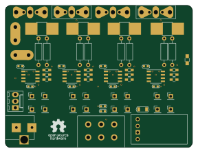
High current 1
71.8 × 54.6 mm66 parts2LCC-BY-4.00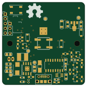
Esp32 button
44 × 44 mm56 parts2LCC-BY-4.00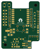 ESP8266
Esp8266 button
40 × 50 mm35 parts2LCC-BY-4.00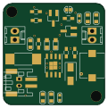
Tp5410 breakout
30 × 30 mm27 parts2LCC-BY-4.00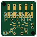
Simple step load
30 × 30 mm19 parts2LCC-BY-4.00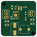
Mp2303 breakout
30 × 30 mm18 parts2LCC-BY-4.00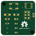 AVR/Arduino
Smd class
30 × 30 mm16 parts2LCC-BY-4.00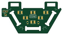
Led board
55.4 × 29.5 mm13 parts2LCC-BY-4.00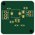
Sx1308 breakout
30 × 30 mm11 parts2LCC-BY-4.00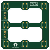
Square grid board
50 × 50 mm11 parts2LCC-BY-4.00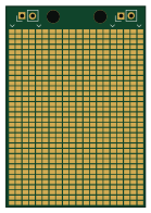
Smd proto
34 × 49 mm6 parts2LCC-BY-4.00
Similar boards
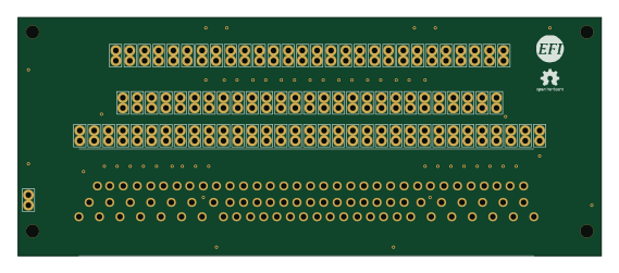
88 Pin Vag Breakout
rusefi
142 × 58 mm91 parts2LGPL-3.01.2k
134pin 7-967288-1
139.7 × 73.7 mm38 parts2LGPL-3.01.2k
Breakout 60pin EEC-IV
139.7 × 62.2 mm15 parts2LGPL-3.01.2k
Breakout 112pin Connector
174 × 58 mm39 parts2LGPL-3.01.2k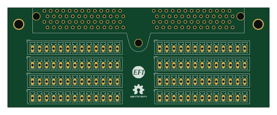
Eecv breakout
140.8 × 53.7 mm9 parts4LGPL-3.01.2k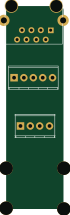
Rj45 breakout
rene-dev
15.2 × 53.8 mm3 parts2LGPL-3.0979