
Devbackup

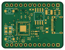
About the Devbackup PCB
Devbackup is an open source RP2040/RP2350 PCB design by espcaa, published on GitHub. It is a 2-layer board measuring 33.6 × 25.4 mm, with 41 components from 20 distinct parts.
Its main chip is the RP2350A-QFN60, from the RP2040/RP2350 family. Other key parts include the AP63203WU-7, GT-USB-7010ASV, W25Q64JVSSIQ_C179171 and ABM8-272-T3_C20625731. By type, the board carries 22 capacitors, 8 resistors, 5 ICs, 2 connectors, 2 switches and 2 inductors.
It belongs with the dev boards & breakouts designs in this gallery.
From the project
a rp2350 based devboard with mechanical switches!
This is a devboard based on the RP2350 chip (the rp2040's successor) with three mechanical switches, with every gpio exposed on pin headers + extras like 3v3 and vbus. It was entirely designed in Kicad and everything is open source! 4 layer board that can be manufactured with normal jlcpcb tolerances.\ \
- RP2350 - 3x Cherry MX switches - Recommended abracon crystal & inductors - AP63203WU-7 for the 5v to 3v3 conversion - 1x23 pin headers - W25Q64JVSSIQ_C179171 chip for the flash (64mb) - a usb-c connector
Main components on the Devbackup
Devbackup bill of materials (BOM)
41 components, 20 distinct parts — part numbers from the project's BOM.
| Qty | Part | Footprint | Refs |
|---|---|---|---|
| 1 | AP63203WU-7 | TSOT-26_L2.9-W1.6-P0.95-LS2.8-BL | U1 |
| 1 | GT-USB-7010ASV | USB-C-SMD_G-SWITCH_GT-USB-7010ASV | U2 |
| 1 | W25Q64JVSSIQ_C179171 | SOIC-8_L5.3-W5.3-P1.27-LS8.0-BL | U4 |
| 1 | ABM8-272-T3_C20625731 | CRYSTAL-SMD_4P-L3.2-W2.5-BL | U5 |
| 1 | RP2350A-QFN60 | QFN-60-1EP_7x7mm_P0.4mm_EP3.4x3.4mm | U6 |
| 2 | CONN_01X23_PIN Conn_01x12_Pin | PinHeader_1x12_P2.54mm_Vertical | J1, J2 |
| 2 | SW_Push | SW-SMD_L3.9-W3.0-P4.45 | SW1, SW2 |
| 1 | 3.9UH 47uh | L_1210_3225Metric | L1 |
| 1 | 3.3U 3.3u | 0603-special | L2 |
| 1 | 10UF 10uf | C_0805_2012Metric | C1 |
| 1 | 100NF 100nf | C_0402_1005Metric | C2 |
| 2 | 22UF 22uf | C_0603_1608Metric | C3, C4 |
| 3 | 4.7U 4.7u | C_0402_1005Metric_small_pads | C5, C6, C7 |
| 13 | 100N 100n | C_0402_1005Metric | C8, C9, C10, C11, C13, C14, C15, C16 +5 |
| 2 | 15P 15p | C_0402_1005Metric | C23, C24 |
| 1 | 5.1K 5.1k | R_0402_1005Metric | R1 |
| 1 | 33 | R_0402_1005Metric | R2 |
| 1 | 10K 10k | R_0402_1005Metric | R3 |
| 3 | 1k | R_0402_1005Metric | R4, R5, R8 |
| 2 | 27 | R_0402_1005Metric | R6, R7 |
Devbackup design files
The KiCad project lives in the espcaa/clicky-devboard repository on GitHub; these links point at the commit this page was built from.
Devbackup: common questions
What microcontroller does the Devbackup use?
The Devbackup is built around the RP2350A-QFN60, from the RP2040/RP2350 family.
How big is the Devbackup PCB?
The Devbackup measures 33.6 × 25.4 mm, has 2 copper layers and is 1.6 mm thick.
How many components are on the Devbackup?
41 components, from 20 distinct parts, with part numbers taken from the project's own BOM. The full bill of materials is listed on this page.
Where can I download the Devbackup design files?
From the espcaa/clicky-devboard repository on GitHub, which has the KiCad layout and the BOM; the links under Design files point to each one.
Can I use the Devbackup design in my own project?
The repository has no license, so all rights stay with espcaa. Use it as a reference, and ask the author before reusing the design.
Can I test firmware for the Devbackup without the hardware?
Yes. HardLabs builds a simulation of the board from its netlist and BOM, so you can run and debug RP2040/RP2350 firmware against it before you order a PCB.
More boards in clicky-devboard
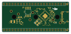
Similar boards
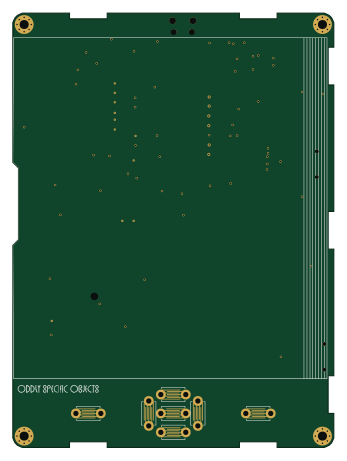 RP2040/RP2350
Open Book Abridged Edition
joeycastillo
85 × 115 mm29 parts2LCC-BY-SA-4.08.1k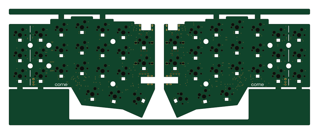 RP2040/RP2350
Corne
foostan
277.2 × 107.5 mm164 parts2LCC-BY-4.07.7k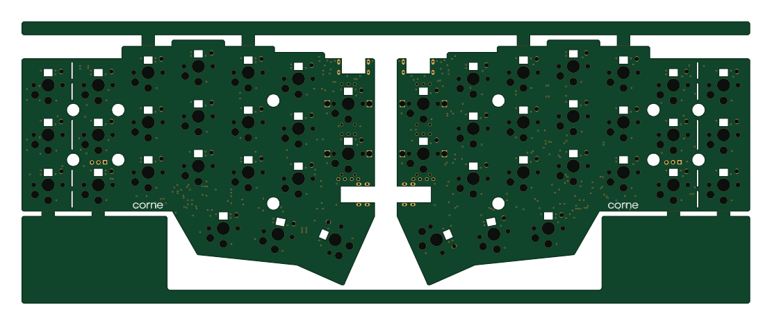 RP2040/RP2350
Corne
277.2 × 107.5 mm164 parts2LCC-BY-4.07.7k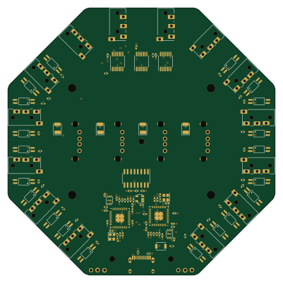 RP2040/RP2350
Hid remapper
jfedor2
100 × 100 mm124 parts2LMIT1.7k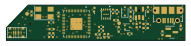 RP2040/RP2350
Msa
Mentra-Community
47.8 × 9.4 mm53 parts2LMIT1.2k RP2040/RP2350
Open Source Smart Glasses
93 × 10.5 mm80 parts4LMIT1.2k