
DaisyDelayHardwareTestRoute


About the DaisyDelayHardwareTestRoute PCB
DaisyDelayHardwareTestRoute is an open source PCB design by fablabnk, published on GitHub. It is a 2-layer board measuring 30 × 128.5 mm, with 49 components from 25 distinct parts.
Other key parts include the TL074, MCP6002, MCP6002-xP and Electrosmith_Daisy_Seed_Rev4. By type, the board carries 20 resistors, 16 capacitors, 5 connectors, 3 ICs, 1 module and 1 switch.
It belongs with the audio designs in this gallery.
From the project
This repo documents the hardware design of a Daisy Seed-based Eurorack module called the Daisy Delay and contains the KiCad files for the project.
This repo documents the hardware design of a Daisy Seed-based Eurorack module called the Daisy Delay and contains the KiCad files for the project.
The Daisy Delay is planned as simple 6HP mono delay-line module, but can easily be used as a development platform for any kind of single-in/single-out audio processor.
This README gives an overview of the project, but there are also seperate notes for the schematic and the PCB.
Main components on the DaisyDelayHardwareTestRoute
DaisyDelayHardwareTestRoute bill of materials (BOM)
49 components, 25 distinct parts — part numbers from the project's BOM.
| Qty | Part | Footprint | Refs |
|---|---|---|---|
| 1 | TL074 | DIP-14_W7.62mm | U2 |
| 1 | MCP6002 LM4040DBZ-10 | TO-92_Inline_Wide | U3 |
| 1 | MCP6002-xP | DIP-8_W7.62mm | U4 |
| 1 | Electrosmith_Daisy_Seed_Rev4 | Electrosmith_Daisy_Seed | A1 |
| 1 | AUDIO_OUTPUT | PJ301M-12_T_S | J1 |
| 1 | FEEDBACK_CV_INPUT | PJ301M-12_T_S | J2 |
| 1 | DELAY_TIME_CV_INPUT | PJ301M-12_T_S | J3 |
| 1 | EURO_PWR_2x8 | PinHeader_2x08_P2.54mm_Vertical | J4 |
| 1 | AUDIO_INPUT | PJ301M-12_T_S | J5 |
| 1 | DELAY_TIME_POT_10K | Alpha9mmPot | RV1 |
| 1 | FEEDBACK_POT_10K | Alpha9mmPot | RV2 |
| 1 | SW_SPDT | SolderWire-0.5sqmm_1x02_P4.6mm_D0.9mm_OD2.1mm | SW1 |
| 1 | LED | LED_D5.0mm | D1 |
| 2 | 103 10nF | C_Disc_D3.0mm_W1.6mm_P2.50mm | C1, C6 |
| 3 | 470 47PF | C_Disc_D3.0mm_W1.6mm_P2.50mm | C2, C4, C5 |
| 1 | 561 560PF | C_Disc_D3.0mm_W1.6mm_P2.50mm | C3 |
| 6 | 104 100nF | C_Disc_D3.0mm_W1.6mm_P2.50mm | C7, C8, C9, C10, C13, C14 |
| 3 | 103 10µF | C_Disc_D3.0mm_W1.6mm_P2.50mm | C11, C12, C15 |
| 1 | 104 220µF | CP_Radial_D5.0mm_P2.50mm | C16 |
| 2 | 200K | R_Axial_DIN0204_L3.6mm_D1.6mm_P5.08mm_Horizontal | R1, R15 |
Show 5 more
| Qty | Part | Footprint | Refs |
|---|---|---|---|
| 8 | 100K | R_Axial_DIN0204_L3.6mm_D1.6mm_P5.08mm_Horizontal | R2, R5, R6, R8, R11, R12, R13, R16 |
| 4 | 66.5K | R_Axial_DIN0204_L3.6mm_D1.6mm_P5.08mm_Horizontal | R3, R4, R17, R18 |
| 3 | 1K | R_Axial_DIN0204_L3.6mm_D1.6mm_P5.08mm_Horizontal | R7, R14, R20 |
| 2 | 10K | R_Axial_DIN0204_L3.6mm_D1.6mm_P5.08mm_Horizontal | R9, R10 |
| 1 | 2K | R_Axial_DIN0204_L3.6mm_D1.6mm_P5.08mm_Horizontal | R19 |
DaisyDelayHardwareTestRoute design files
The KiCad project lives in the fablabnk/DaisyDelayHardware repository on GitHub; these links point at the commit this page was built from.
DaisyDelayHardwareTestRoute: common questions
How big is the DaisyDelayHardwareTestRoute PCB?
The DaisyDelayHardwareTestRoute measures 30 × 128.5 mm, has 2 copper layers and is 1.6 mm thick.
How many components are on the DaisyDelayHardwareTestRoute?
49 components, from 25 distinct parts, with part numbers taken from the project's own BOM. The full bill of materials is listed on this page.
Where can I download the DaisyDelayHardwareTestRoute design files?
From the fablabnk/DaisyDelayHardware repository on GitHub, which has the KiCad layout and the BOM; the links under Design files point to each one.
Can I use the DaisyDelayHardwareTestRoute design in my own project?
The repository has no license, so all rights stay with fablabnk. Use it as a reference, and ask the author before reusing the design.
More boards in DaisyDelayHardware

Similar boards
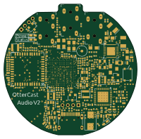
OtterCastAudioV2
Ottercast
50 × 49.3 mm216 parts4LMIT665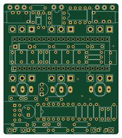
FunBox
GuitarML
59.7 × 67.5 mm63 parts2LMIT278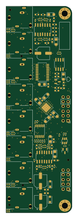
Eurorack pmod
apfaudio
35 × 110 mm116 parts4LCERN-OHL-S-2.0239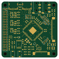
XassetteAsterisk
SdtElectronics
56 × 56 mm137 parts2LCERN-OHL-W-2.0229
AddOnC
freeDSP
380 × 45 mm97 parts2LCC-BY-SA-4.0222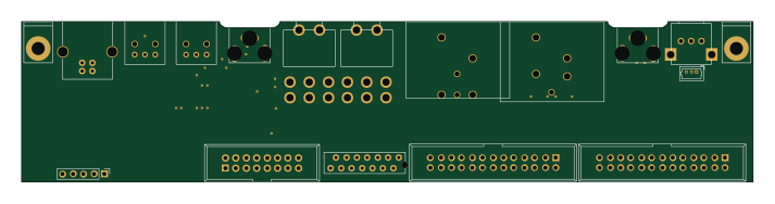
AddOnA
178 × 39 mm55 parts2LCC-BY-SA-4.0222