
Photodiode lab

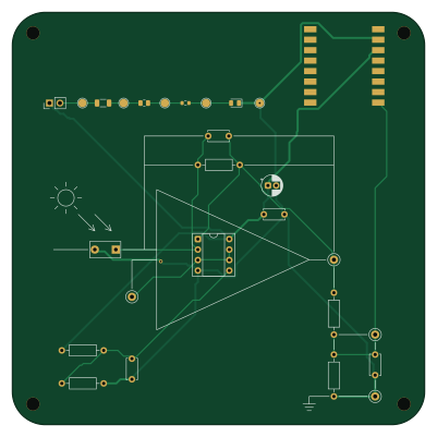
About the Photodiode lab PCB
Photodiode lab is an open source ESP32 PCB design by fborello-lambda, published on GitHub. It is a 2-layer board measuring 100 × 100 mm, with 22 components from 22 distinct parts.
Its main chip is the ESP32-C3 SuperMini, from the ESP32 family. Other key parts include the MCP6002-I/P. By type, the board carries 7 resistors, 4 test points, 4 capacitors, 2 ICs, 2 diodes and 1 jumper.
From the project
🔌 PCBs made with LLMs
This is a 3.3 V teaching transimpedance amplifier (TIA) for a Vishay BPW34, an MCP6002-I/P in an 8-pin DIP socket, and the shared direct-solder ESP32-C3 footprint. The ESP32-C3 GPIO0 ADC input is ADCOUT`.
Fit the BPW34 in the marked top-view orientation: pad 1 (K, cathode) goes to the MCP6002 A inverting input, net SUM; pad 2 (anode) goes to GND. On the PCB, K is on the right and the anode on the left. The photodiode is therefore reverse biased at about 1.65 V. The MCP6002 DIP-8 pinout is: 1 OUTA=VOUT, 2 INA−=SUM, 3 INA+=VREF, 4 VSS=GND, 5 INB+=REFDIV, 6 INB−=VREF, 7 OUTB=VREF, 8 VDD=+3V3`.
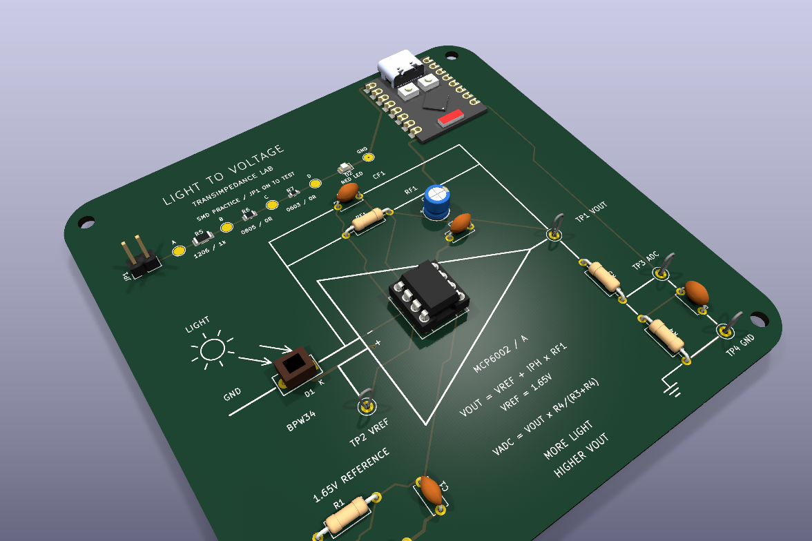
Main components on the Photodiode lab
Photodiode lab bill of materials (BOM)
22 components, 22 distinct parts — part numbers from the project's BOM.
| Qty | Part | Footprint | Refs |
|---|---|---|---|
| 1 | ESP32-C3 SuperMini | ESP32-C3-SuperMini | U1 |
| 1 | MCP6002-I/P | U2 | U2 |
| 1 | 1n C0G | CF1 | CF1 |
| 1 | PRACTICE ENABLE | JP1 | JP1 |
| 1 | 100k 1% | RF1 | RF1 |
| 1 | VOUT | TP1 | TP1 |
| 1 | VREF | TP2 | TP2 |
| 1 | ADC_OUT | TP3 | TP3 |
| 1 | GND | TP4 | TP4 |
| 1 | BPW34 | D1 | D1 |
| 1 | RED | D2 | D2 |
| 1 | 100N 100n | C1 | C1 |
| 1 | 100N 100n | C2 | C2 |
| 1 | 10u / 10V | C3 | C3 |
| 1 | 100N 100n | C4 | C4 |
| 1 | 10k 1% | R1 | R1 |
| 1 | 10k 1% | R2 | R2 |
| 1 | 10k 1% | R3 | R3 |
| 1 | 22k 1% | R4 | R4 |
| 1 | 1k | R5 | R5 |
Show 2 more
| Qty | Part | Footprint | Refs |
|---|---|---|---|
| 1 | 0R | R6 | R6 |
| 1 | 0R | R7 | R7 |
Photodiode lab design files
The KiCad project lives in the fborello-lambda/pcbs_llm_driven_design repository on GitHub; these links point at the commit this page was built from.
Photodiode lab: common questions
What microcontroller does the Photodiode lab use?
The Photodiode lab is built around the ESP32-C3 SuperMini, from the ESP32 family.
How big is the Photodiode lab PCB?
The Photodiode lab measures 100 × 100 mm, has 2 copper layers and is 1.6 mm thick.
How many components are on the Photodiode lab?
22 components, from 22 distinct parts, with part numbers taken from the project's own BOM. The full bill of materials is listed on this page.
Where can I download the Photodiode lab design files?
From the fborello-lambda/pcbs_llm_driven_design repository on GitHub, which has the KiCad layout, the schematic and the BOM; the links under Design files point to each one.
Can I use the Photodiode lab design in my own project?
The repository has no license, so all rights stay with fborello-lambda. Use it as a reference, and ask the author before reusing the design.
Can I test firmware for the Photodiode lab without the hardware?
Yes. HardLabs builds a simulation of the board from its netlist and BOM, so you can run and debug ESP32 firmware against it before you order a PCB.
More boards in pcbs_llm_driven_design
Similar boards
 ESP32
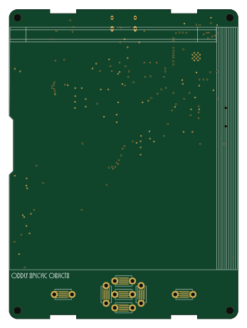
ESP32Open Book Abridged Edition
joeycastillo
85 × 115 mm65 parts2LCC-BY-SA-4.08.1k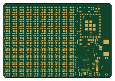 ESP32
ESP32Badge
atopile
56.3 × 39 mm239 parts4LMIT4.0k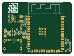 ESP32
ESP32Esp32 minimal
36.2 × 26.8 mm20 parts2LMIT4.0k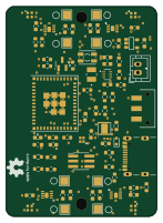 ESP32
ESP32Racer
StuckAtPrototype
36 × 50.2 mm70 parts4LApache-2.03.8k ESP32
ESP32Controller
29 × 74 mm58 parts4LApache-2.03.8k ESP32
ESP32Bitaxe
skot
56.5 × 99.8 mm86 parts4LCERN-OHL-S-2.01.4k