
Clock

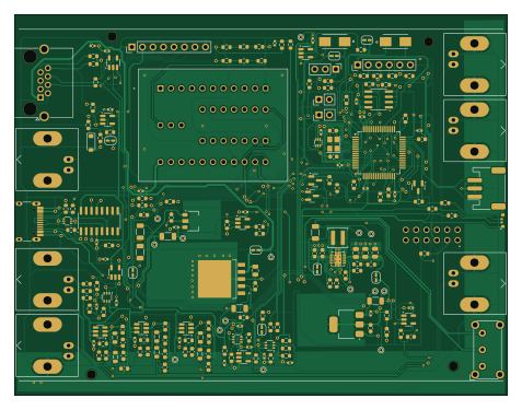
About the Clock PCB
Clock is an open source STM32 PCB design by fluffy, published on GitHub under the BSD-3-Clause license. It is a 2-layer board measuring 119 × 92 mm, with 192 components from 62 distinct parts.
Its main chip is the STM32F405RGTX, from the STM32 family. Other key parts include the ADA4807-1, SN74LVC1G14DBV, TLV3603DCKR, L78L05_SOT89 and AMS1117-3.3. By type, the board carries 80 resistors, 63 capacitors, 22 ICs, 9 connectors, 8 inductors and 4 switches.
From the project
Blinking lights to tell time
If the schematic or boards in changed such that the software can tell the difference, the rev need to go up a letter. Other changes can get a sub number on the rev letter.
Don't update sybols / footprint from libraries. It over writes stuff.
When done, do a plot to generate schematic in production subdir.
When done, do an export of step to generate a model in production subdir.
Main components on the Clock
Clock bill of materials (BOM)
192 components, 62 distinct parts — part numbers from the project's BOM.
| Qty | Part | Footprint | Refs |
|---|---|---|---|
| 3 | ADA4807-1 | SOT-23-6 | U1, U4, U5 |
| 7 | SN74LVC1G14DBV | SOT-23-5 | U2, U3, U7, U17, U19, U20, U21 |
| 3 | TLV3603DCKR | SOT-363_SC-70-6 | U6, U8, U16 |
| 1 | L78L05_SOT89 | SOT-89-3 | U9 |
| 1 | STM32F405RGTX STM32F405RGTx | LQFP-64_10x10mm_P0.5mm | U10 |
| 1 | AMS1117-3.3 | SOT-223-3_TabPin2 | U11 |
| 1 | BA50DD0WHFP BA50DD0WHFP-TR | DPAK172P1054X200-6N | U12 |
| 1 | M24C02-RMN | SOIC-8_3.9x4.9mm_P1.27mm | U13 |
| 1 | CH340C | SOIC-16_3.9x9.9mm_P1.27mm | U14 |
| 1 | USBLC6-2P6 | SOT-666 | U15 |
| 1 | TMP112AIDRLR | SOT-563 | U18 |
| 1 | TPS63060 | Texas_S-PWSON-N10_ThermalVias-CJ | U23 |
| 3 | 2N7002 | SOT-23 | Q1, Q9, Q10 |
| 1 | 16MHZ 16MHz | Crystal_SMD_3225-4Pin_3.2x2.5mm | Y2 |
| 1 | RJ45 | RJ45_Amphenol_RJHSE5380 | J1 |
| 1 | CONN_01X03 Conn_01x03 | JST_PH_S3B-PH-SM4-TB_1x03-1MP_P2.00mm_Horizontal | J2 |
| 6 | KH-BNC50-3511 | BNC_Amphenol_B6252HB-NPP3G-50_Horizontal-CJ | J3, J7, J9, J10, J11, J13 |
| 1 | C165948 USB_C_Receptacle | USB_C_Receptacle_HRO_TYPE-C-31-M-12 | J4 |
| 2 | 147873-2 | SW_147873-2 | S1, S3 |
| 1 | SW_PUSH_4PDT SW_Push_4PDT | PBH4UOANAGX | SW1 |
Show 42 more
| Qty | Part | Footprint | Refs |
|---|---|---|---|
| 1 | C273395 SW_SPDT | SW_E-Switch_EG1224_SPDT_Angled | SW2 |
| 1 | C8598 B5819W SL | D_SOD-123 | D4 |
| 1 | MHS110FRGBCT LED_ABGR | LED_RGB_MHS110FRGBCT | D5 |
| 1 | C127301 120Ω@100MHz | R_0603_1608Metric | FB1 |
| 6 | 1UH 1uH | L_0805_2012Metric | L1, L2, L3, L4, L5, L6 |
| 1 | XFL4020-152MEC 1.5uH | L_Coilcraft_XAL4020-XXX | L7 |
| 29 | 100N 100n | C_0402_1005Metric | C1, C2, C9, C10, C11, C17, C18, C25 +21 |
| 3 | 1N0 1n0 | C_0603_1608Metric | C3, C16, C21 |
| 1 | 47P 47p | C_0603_1608Metric | C4 |
| 6 | 150P 150p | C_0603_1608Metric | C5, C7, C12, C14, C19, C23 |
| 3 | 220P 220p | C_0603_1608Metric | C6, C15, C22 |
| 3 | 330P 330p | C_0603_1608Metric | C8, C13, C20 |
| 5 | 100N 100n | C_0603_1608Metric | C24, C27, C37, C54, C63 |
| 2 | 33P 33p | C_0603_1608Metric | C28, C29 |
| 4 | 10U 10u | C_0603_1608Metric | C34, C43, C60, C62 |
| 3 | 2U2 2u2 | C_0603_1608Metric | C35, C40, C42 |
| 4 | 22U 22u | C_0805_2012Metric | C41, C61, C64, C65 |
| 3 | 100R | R_0603_1608Metric | R1, R46, R47 |
| 3 | 510R | R_0603_1608Metric | R2, R6, R10 |
| 3 | 49R9 | R_0603_1608Metric | R3, R7, R11 |
| 1 | 200R | R_0603_1608Metric | R4 |
| 30 | 1K0 | R_0603_1608Metric | R5, R19, R20, R22, R24, R29, R30, R39 +22 |
| 3 | 270R | R_0603_1608Metric | R8, R25, R48 |
| 1 | 2R0 | R_0603_1608Metric | R9 |
| 4 | 1K5 | R_0603_1608Metric | R12, R13, R58, R59 |
| 1 | 330R | R_0603_1608Metric | R14 |
| 2 | C17901 100R 250mW | R_1206_3216Metric | R15, R16 |
| 1 | 20R | R_0603_1608Metric | R17 |
| 3 | 130K | R_0603_1608Metric | R18, R21, R45 |
| 1 | 22K | R_0603_1608Metric | R23 |
| 1 | 22R0 | R_0603_1608Metric | R26 |
| 5 | 47K | R_0603_1608Metric | R27, R28, R76, R77, R78 |
| 1 | 120K | R_0603_1608Metric | R31 |
| 4 | 4K7 | R_0603_1608Metric | R32, R33, R34, R36 |
| 1 | 3K3 | R_0603_1608Metric | R35 |
| 2 | 5K1 | R_0603_1608Metric | R37, R38 |
| 1 | 0R020 | R_1206_3216Metric | R42 |
| 1 | 10K | R_0603_1608Metric | R50 |
| 2 | 12K | R_0603_1608Metric | R53, R75 |
| 1 | 150R | R_0603_1608Metric | R70 |
| 2 | 47R | R_0603_1608Metric | R73, R74 |
| 3 | 0R1 | R_1206_3216Metric | R79, R81, R82 |
Clock design files
The KiCad project lives in the fluffy/blinky repository on GitHub; these links point at the commit this page was built from.
Clock: common questions
What microcontroller does the Clock use?
The Clock is built around the STM32F405RGTX, from the STM32 family.
How big is the Clock PCB?
The Clock measures 119 × 92 mm, has 2 copper layers and is 1.6 mm thick.
How many components are on the Clock?
192 components, from 62 distinct parts, with part numbers taken from the project's own BOM. The full bill of materials is listed on this page.
Where can I download the Clock design files?
From the fluffy/blinky repository on GitHub, which has the KiCad layout, the schematic and the BOM; the links under Design files point to each one.
Can I use the Clock design in my own project?
Yes, under the terms of its BSD-3-Clause license, which fluffy chose for the repository.
Can I test firmware for the Clock without the hardware?
Yes. HardLabs builds a simulation of the board from its netlist and BOM, so you can run and debug STM32 firmware against it before you order a PCB.
More boards in blinky
Similar boards
 STM32
STM32LumenPnP Motherboard
opulo-inc
149 × 95 mm296 parts4LCC-BY-SA-4.03.7k STM32
STM32AxxSolder
AxxAxx
39 × 82.5 mm122 parts2LGPL-3.01.7k STM32
STM32LibreVNA
jankae
122 × 98 mm592 parts6LGPL-3.01.6k STM32
STM32AIOC
skuep
21 × 31.5 mm47 parts2LMIT1.4k STM32
STM32Ferris
pierrechevalier83
208.8 × 86.8 mm102 parts2LSHL-2.11.3k STM32
STM32176 pin board
rusefi
61.8 × 73.2 mm76 parts2LGPL-3.01.2k