
Sp02 monitor

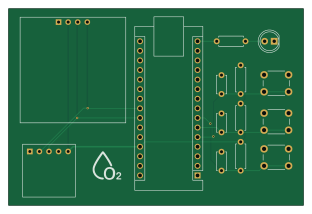
About the Sp02 monitor PCB
Sp02 monitor is an open source AVR/Arduino PCB design by hammadurrehman2006, published on GitHub. It is a 4-layer board measuring 78 × 52 mm, with 10 components from 5 distinct parts.
Its main chip is the Arduino_Nano_v3.x, from the AVR/Arduino family. Other key parts include the MAX30102 and SSD1306. By type, the board carries 4 resistors, 3 capacitors, 2 ICs and 1 module.
It belongs with the displays & leds designs in this gallery.
From the project
A collection of KiCad PCB designs developed during my Electronic Engineering degree (2024-28). Includes university projects, personal experiments, and custom components—featuring schematics, layouts, Gerber files, and documentation. Open-source hardware for education, collaboration, and real-world manufacturing.
This is my first custom PCB project — a compact SP02 Monitoring Device built using:
- ✅ MAX30102 – Pulse oximeter and heart rate sensor - ✅ SSD1306 OLED Display – For real-time oxygen and pulse display - ✅ Arduino Nano – Acts as the main controller - ✅ KiCad 9.0 – Used for schematic, layout, and Gerber generation
- Live display of SPO2 and heart rate on OLED - Compact 2-layer PCB layout - Custom footprints and symbols designed in KiCad - Beginner-friendly open-source hardware
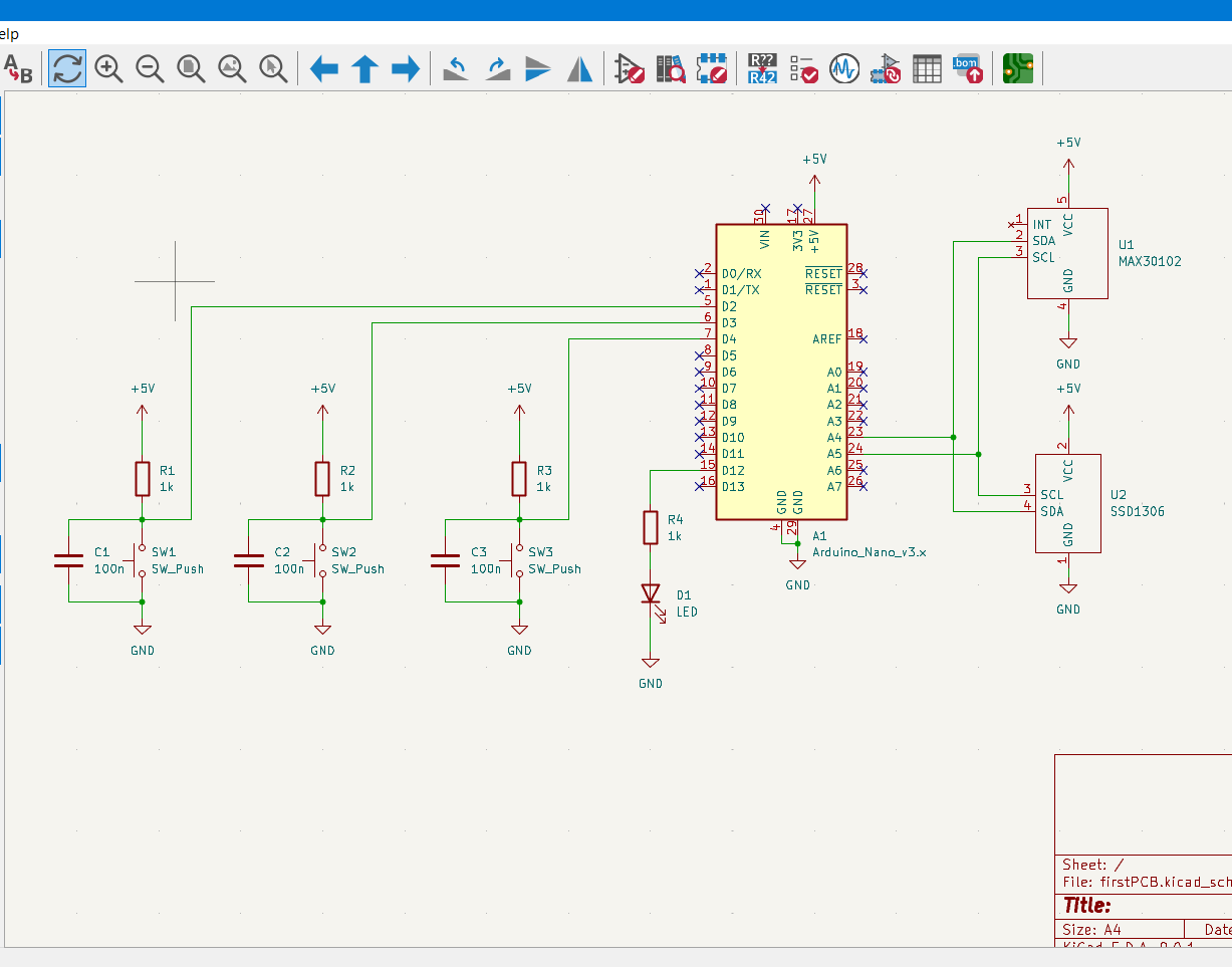
Main components on the Sp02 monitor
Sp02 monitor bill of materials (BOM)
10 components, 5 distinct parts.
| Qty | Part | Footprint | Refs |
|---|---|---|---|
| 1 | MAX30102 | MAX30102_MODULE | U1 |
| 1 | SSD1306 | SSD1306 | U2 |
| 1 | Arduino_Nano_v3.x | Arduino_Nano | A1 |
| 3 | 100n | C_Disc_D4.7mm_W2.5mm_P5.00mm | C1, C2, C3 |
| 4 | 1k | R_Axial_DIN0207_L6.3mm_D2.5mm_P7.62mm_Horizontal | R1, R2, R3, R4 |
Sp02 monitor design files
The KiCad project lives in the hammadurrehman2006/kicad_lab repository on GitHub; these links point at the commit this page was built from.
Sp02 monitor: common questions
What microcontroller does the Sp02 monitor use?
The Sp02 monitor is built around the Arduino_Nano_v3.x, from the AVR/Arduino family.
How big is the Sp02 monitor PCB?
The Sp02 monitor measures 78 × 52 mm, has 4 copper layers and is 1.600198 mm thick.
How many components are on the Sp02 monitor?
10 components, from 5 distinct parts. The full bill of materials is listed on this page.
Where can I download the Sp02 monitor design files?
From the hammadurrehman2006/kicad_lab repository on GitHub, which has the KiCad layout and the schematic; the links under Design files point to each one.
Can I use the Sp02 monitor design in my own project?
The repository has no license, so all rights stay with hammadurrehman2006. Use it as a reference, and ask the author before reusing the design.
Can I test firmware for the Sp02 monitor without the hardware?
Yes. HardLabs builds a simulation of the board from its netlist and BOM, so you can run and debug AVR/Arduino firmware against it before you order a PCB.
More boards in kicad_lab
 STM32
STM32STM32 gps tracker
46 × 60.3 mm53 parts4LNo license1
Sine wave inverter
91.4 × 54.6 mm39 parts2LNo license1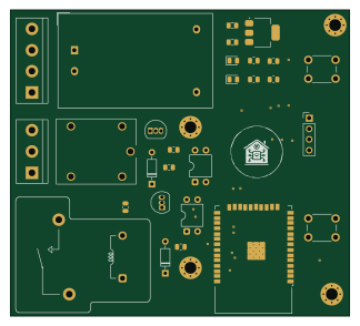 ESP32
ESP3230A home automation using esp32
80.8 × 73.1 mm28 parts2LNo license1
Usb to uart
31.7 × 15 mm19 parts2LNo license1
Transformerless power supply
55.4 × 40.6 mm18 parts2LNo license1
Dc motor speed controller
60.7 × 30.2 mm15 parts2LNo license1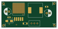
Dc boost converter
47.6 × 22.5 mm13 parts2LNo license1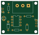
Servo tester
32.7 × 29.6 mm10 parts2LNo license1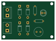
Ac to dc converter
47.5 × 34 mm10 parts2LNo license1
Motor driver
24 × 16.3 mm8 parts2LNo license1
Similar boards
 AVR/Arduino
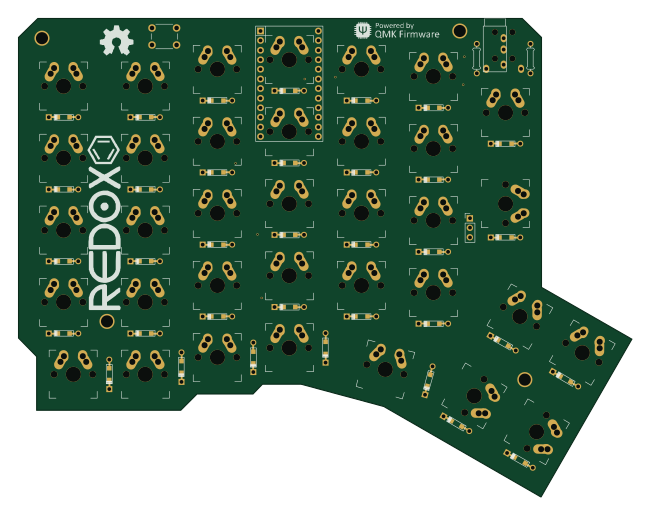
Redox keyboard
mattdibi
162.2 × 126.5 mm77 parts2LMIT2.0k AVR/Arduino
ModuleV450
stuartpittaway
30 × 61.4 mm39 parts2LCC-BY-NC-4.01.1k AVR/Arduino
V4
30 × 50 mm38 parts2LCC-BY-NC-4.01.1k AVR/Arduino
Discipline
coseyfannitutti
304.9 × 122.8 mm170 parts2LCC-BY-NC-4.01.0k AVR/Arduino
Megadesk
gcormier
41.7 × 32.2 mm23 parts2LGPL-3.0818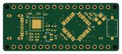 AVR/Arduino
Easyduino Atmega Nano
Hanqaqa
43.4 × 18 mm30 parts4LCERN-OHL-P-2.0746