
UPS-BK-bk

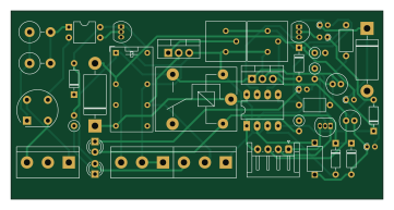
About the UPS-BK-bk PCB
UPS-BK-bk is an open source PCB design by IoTCloudStudio, published on GitHub. It is a 2-layer board measuring 90.2 × 45.7 mm, with 40 components from 29 distinct parts.
Other key parts include the PC817, NE555 and LM7805_TO220. By type, the board carries 11 resistors, 10 diodes, 4 transistors, 4 capacitors, 3 ICs and 2 connectors.
It belongs with the power & battery designs in this gallery.
Main components on the UPS-BK-bk
UPS-BK-bk bill of materials (BOM)
40 components, 29 distinct parts.
| Qty | Part | Footprint | Refs |
|---|---|---|---|
| 1 | PC817 | DIP-4_W7.62mm | U1 |
| 1 | NE555 | DIP-8_W7.62mm_LongPads | U2 |
| 1 | LM7805_TO220 | TO-220-3_Vertical | U3 |
| 1 | IRF540N | TO-220-3_Vertical | Q1 |
| 2 | BC548 | TO-92_Inline | Q2, Q3 |
| 1 | BC557 | TO-92_Inline | Q4 |
| 1 | Conn_01x04 | JST_EH_S4B-EH_1x04_P2.50mm_Horizontal | J1 |
| 1 | 220v | TerminalBlock_bornier-3_P5.08mm | j1 |
| 1 | 0UT | TerminalBlock_bornier-3_P5.08mm | BAT1 |
| 1 | 12V | TerminalBlock_bornier-3_P5.08mm | IN1 |
| 1 | RELEE Simple | Relay_SPDT_SANYOU_SRD_Series_Form_C | K2 |
| 2 | R_POT_TRIM | Potentiometer_Bourns_3386P_Vertical | RV1, RV2 |
| 1 | SW_Push | SW_SPST_CK_RS282G05A3 | SET1 |
| 1 | W10G | Diode_Bridge_Round_D9.8mm | D1 |
| 3 | 1N4148 | D_DO-35_SOD27_P7.62mm_Horizontal | D2, D6, D10 |
| 2 | 1N5408 | D_DO-201AD_P15.24mm_Horizontal | D3, D4 |
| 1 | VERDE | LED_D3.0mm_IRBlack | D5 |
| 1 | ROJO | LED_D3.0mm_IRBlack | D7 |
| 2 | D_Zener | D_DO-35_SOD27_P7.62mm_Horizontal | D8, D9 |
| 1 | 100 Nf | C_Axial_L5.1mm_D3.1mm_P7.50mm_Horizontal | C1 |
Show 9 more
| Qty | Part | Footprint | Refs |
|---|---|---|---|
| 1 | 100nF | C_Axial_L5.1mm_D3.1mm_P7.50mm_Horizontal | C2 |
| 1 | 33u | C_Radial_D5.0mm_H11.0mm_P2.00mm | C3 |
| 1 | 1u | C_Radial_D5.0mm_H11.0mm_P2.00mm | C4 |
| 1 | R | R_Axial_DIN0207_L6.3mm_D2.5mm_P2.54mm_Vertical | R1 |
| 3 | 2K2 | R_Axial_DIN0204_L3.6mm_D1.6mm_P1.90mm_Vertical | R2, R7, R8 |
| 1 | 330 | R_Axial_DIN0204_L3.6mm_D1.6mm_P1.90mm_Vertical | R3 |
| 2 | 68K | R_Axial_DIN0516_L15.5mm_D5.0mm_P5.08mm_Vertical | R4, R5 |
| 1 | 180 | R_Axial_DIN0204_L3.6mm_D1.6mm_P1.90mm_Vertical | R6 |
| 3 | 10k | R_Axial_DIN0207_L6.3mm_D2.5mm_P2.54mm_Vertical | R9, R10, R11 |
UPS-BK-bk design files
The KiCad project lives in the IoTCloudStudio/HW_Develop repository on GitHub; these links point at the commit this page was built from.
UPS-BK-bk: common questions
How big is the UPS-BK-bk PCB?
The UPS-BK-bk measures 90.2 × 45.7 mm, has 2 copper layers and is 1.6 mm thick.
How many components are on the UPS-BK-bk?
40 components, from 29 distinct parts. The full bill of materials is listed on this page.
Where can I download the UPS-BK-bk design files?
From the IoTCloudStudio/HW_Develop repository on GitHub, which has the KiCad layout; the links under Design files point to each one.
Can I use the UPS-BK-bk design in my own project?
The repository has no license, so all rights stay with IoTCloudStudio. Use it as a reference, and ask the author before reusing the design.
More boards in HW_Develop
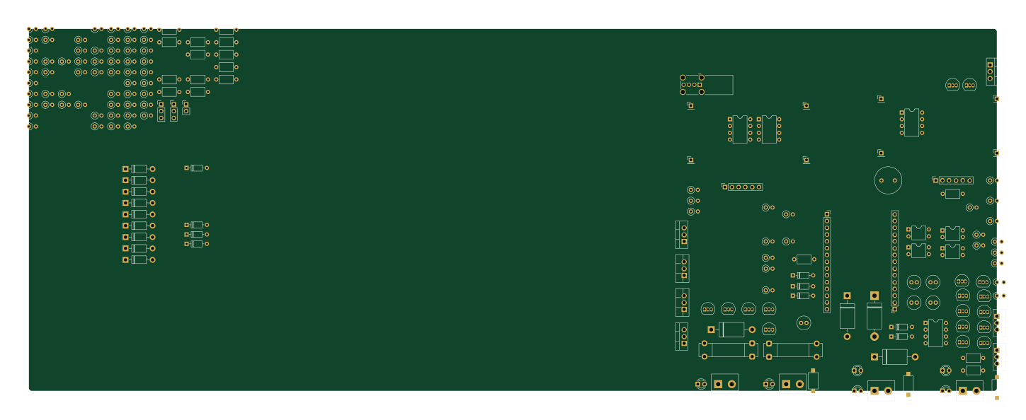
Pcb regulador solar V1.0
361.6 × 135.4 mm187 parts2LNo license1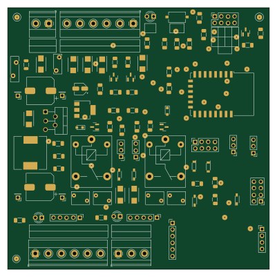 ESP8266
Tesseract
100 × 100 mm87 parts2LNo license1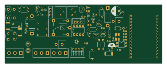 ESP32
UPSV2concepttocheck
135.3 × 51 mm65 parts2LNo license1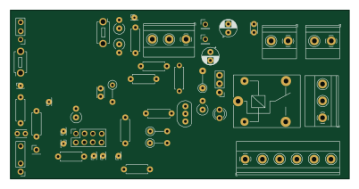 ESP8266
PCB control acceso
100.3 × 50 mm50 parts2LNo license1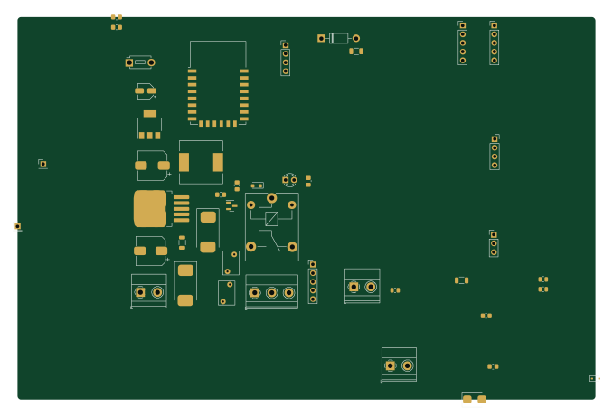 ESP8266
Alarma com
169.3 × 112 mm44 parts2LNo license1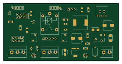 ESP8266
RFW26
100 × 50 mm41 parts2LNo license1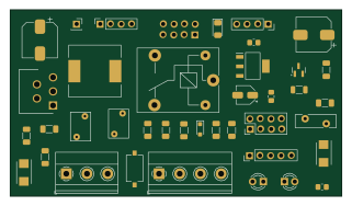 ESP8266
RFW26 2Capas
80 × 45 mm40 parts2LNo license1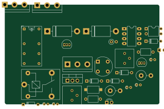
UPS
79.6 × 51.3 mm33 parts2LNo license1
Prueba
66 × 52 mm6 parts2LNo license1 ESP32
RFID FDX Reader
150 × 100 mm6 parts2LNo license1
Similar boards
EinkPDA screen
TalismanDesign
95 × 54 mm27 parts2LApache-2.02.0k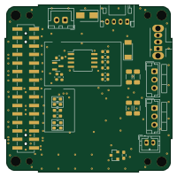
Stack chan
stack-chan
50 × 50 mm33 parts2LApache-2.01.7k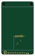
Display Carrier
AxxAxx
35.6 × 58.2 mm5 parts2LGPL-3.01.7k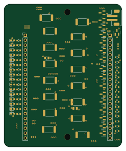
Module 16S PassiveBalanceAddOn
stuartpittaway
61 × 74 mm86 parts2LCC-BY-NC-4.01.1k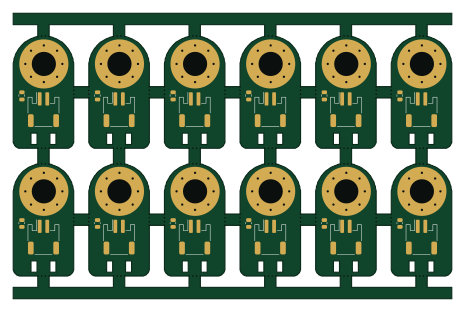
TemperaturePCB PANEL
116 × 75.5 mm178 parts2LCC-BY-NC-4.01.1k
ProgrammingAdapter
10.5 × 83 mm3 parts2LCC-BY-NC-4.01.1k