
Link

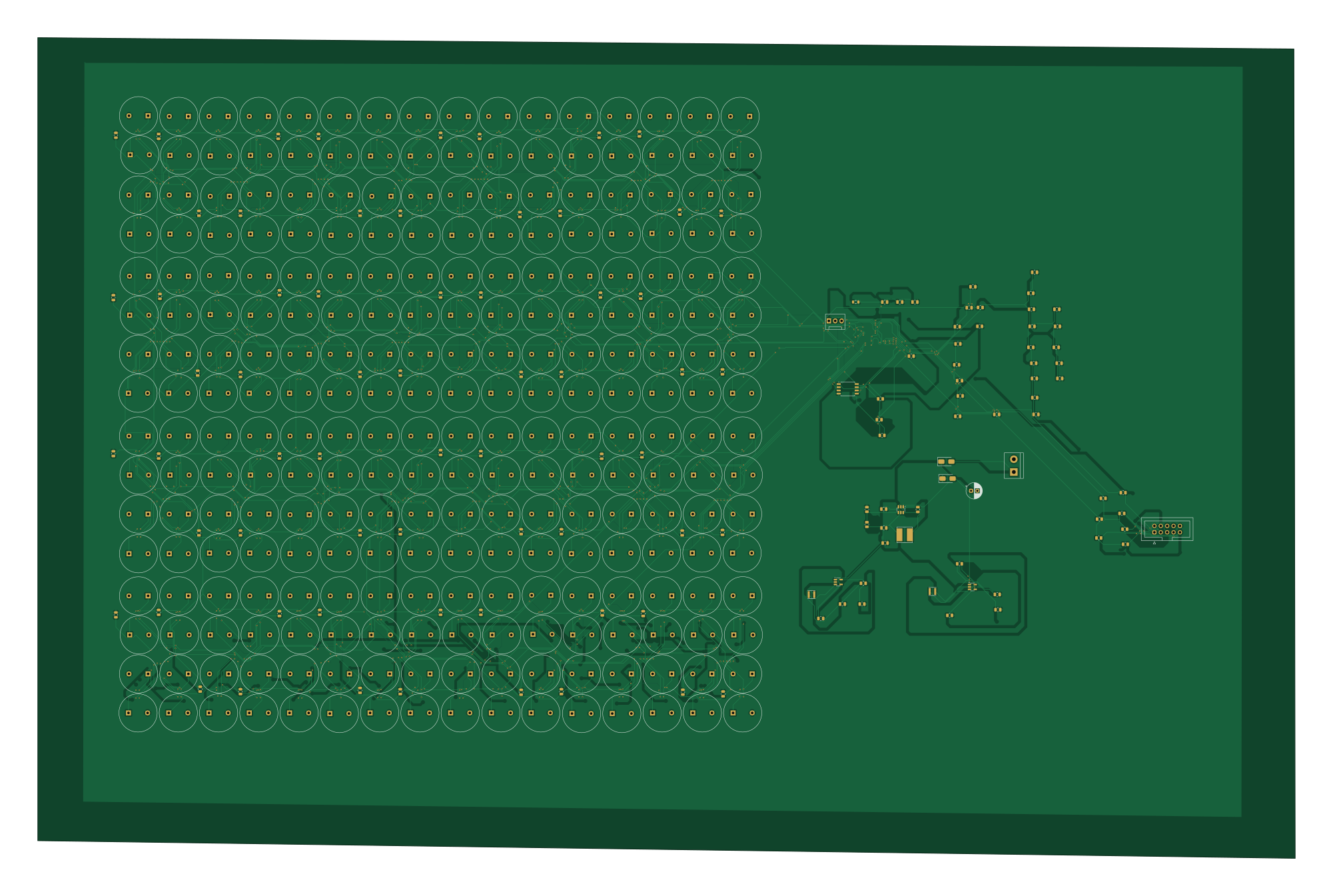
About the Link PCB
Link is an open source FPGA PCB design by Jeo0, published on GitHub. It is a 6-layer board measuring 499.5 × 326 mm, with 548 components from 31 distinct parts.
Its main chip is the LFE5U-25F-6BG256C, from the FPGA family. Other key parts include the 74HC595D, MIC4127YML-TR, W25Q32JVSS, TPS54302 and TLV62569DBV. By type, the board carries 256 speakers, 164 ICs, 99 capacitors, 19 resistors, 4 inductors and 3 connectors.
It belongs with the displays & leds designs in this gallery.
From the project
automatic trajectory generator cross-platform client for acoustic volumetric displays (dis our thesis :))
KiCad Local History Directory =============================
This directory contains automatic snapshots of your project files. KiCad periodically saves copies of your work here, allowing you to recover from accidental changes or data loss.
You can browse and restore previous versions through KiCad's File > Local History menu.
To disable this feature: Preferences > Common > Project Backup > Enable automatic backups
Main components on the Link
Link bill of materials (BOM)
548 components, 31 distinct parts.
| Qty | Part | Footprint | Refs |
|---|---|---|---|
| 32 | 74HC595D | SOIC-16_3.9x9.9mm_P1.27mm | U1, U11, U16, U21, U26, U31, U36, U41 +24 |
| 127 | MIC4127YML-TR | DFN-8-1EP_3x3mm_P0.65mm_EP1.55x2.4mm | U3, U4, U6, U12, U13, U14, U15, U17 +119 |
| 1 | W25Q32JVSS | SOIC-8_5.3x5.3mm_P1.27mm | U7 |
| 1 | TPS54302 | SOT-23-6 | U8 |
| 2 | TLV62569DBV | SOT-23-5 | U9, U10 |
| 1 | LFE5U-25F-6BG256C | LFBGA-289_14x14mm_Layout17x17_P0.8mm | u2 |
| 1 | Conn_01x03_Pin | FanPinHeader_1x03_P2.54mm_Vertical | J1 |
| 1 | JTAG | IDC-Header_2x05_P2.54mm_Vertical | J2 |
| 1 | Screw_Terminal_01x02 | TerminalBlock_bornier-2_P5.08mm | J4 |
| 256 | Speaker_Ultrasound | Buzzer_15x7.5RM7.6 | LS1, LS2, LS3, LS4, LS5, LS6, LS7, LS8 +248 |
| 1 | MIC4127YML-TR | DFN-8-1EP_3x3mm_P0.65mm_EP1.55x2.4mm | Ue1 |
| 1 | SS34 | D_SMA | D1 |
| 1 | SMAJ12A | D_SMA | D2 |
| 1 | 120R | L_0805_2012Metric | FB1 |
| 1 | 4.7μH | L_Bourns_SRN6045TA | L1 |
| 1 | 1μH | L_Taiyo-Yuden_NR-30xx | L2 |
| 1 | 2.2μH | L_Taiyo-Yuden_NR-30xx | L3 |
| 65 | 0.1μF | C_0805_2012Metric | C1, C2, C3, C4, C5, C6, C7, C8 +57 |
| 21 | 100nF | C_0805_2012Metric | C65, C85, C86, C87, C88, C89, C90, C91 +13 |
| 1 | 47μF | CP_Radial_D6.3mm_P2.50mm | C66 |
Show 11 more
| Qty | Part | Footprint | Refs |
|---|---|---|---|
| 8 | 10μF | C_0805_2012Metric | C67, C71, C73, C84, C95, C97, C99, C108 |
| 4 | 22μF | C_0805_2012Metric | C68, C69, C72, C74 |
| 11 | 4.7K | R_0805_2012Metric | R1, R2, R3, R4, R5, R6, R7, R8 +3 |
| 1 | 22R | R_0805_2012Metric | R12 |
| 1 | 1K | R_0805_2012Metric | R13 |
| 1 | 68k | R_0805_2012Metric | R14 |
| 1 | 22k | R_0805_2012Metric | R15 |
| 1 | 12k | R_0805_2012Metric | R16 |
| 1 | 10k | R_0805_2012Metric | R17 |
| 1 | 51k | R_0805_2012Metric | R18 |
| 1 | 16k | R_0805_2012Metric | R19 |
Link design files
The KiCad project lives in the Jeo0/atg-client repository on GitHub; these links point at the commit this page was built from.
Link: common questions
What microcontroller does the Link use?
The Link is built around the LFE5U-25F-6BG256C, from the FPGA family.
How big is the Link PCB?
The Link measures 499.5 × 326 mm, has 6 copper layers and is 1.6 mm thick.
How many components are on the Link?
548 components, from 31 distinct parts. The full bill of materials is listed on this page.
Where can I download the Link design files?
From the Jeo0/atg-client repository on GitHub, which has the KiCad layout and the schematic; the links under Design files point to each one.
Can I use the Link design in my own project?
The repository has no license, so all rights stay with Jeo0. Use it as a reference, and ask the author before reusing the design.
Can I test firmware for the Link without the hardware?
Yes. HardLabs builds a simulation of the board from its netlist and BOM, so you can run and debug FPGA firmware against it before you order a PCB.
More boards in atg-client
Similar boards
 FPGA
FPGABase board
GlasgowEmbedded
80 × 49 mm222 parts4L0BSD2.2k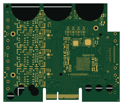 FPGA
FPGAThunderscope Rev5.3
EEVengers
122.5 × 103.5 mm817 parts6LMIT1.3k FPGA
FPGAUsb sniffer
ataradov
58.2 × 38.1 mm86 parts2LBSD-3-Clause1.3k FPGA
FPGATomu, I'm
theacodes
13 × 9.4 mm40 parts4LMIT1.1k FPGA
FPGAIcepi zero
cheyao
65 × 30 mm143 parts4LSHL-2.1828 FPGA
FPGASd2snes
mrehkopf
101.5 × 83 mm147 partsGPL-2.0717