
WLED PCB V2

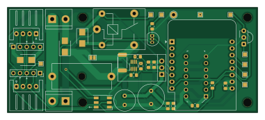
About the WLED PCB V2
WLED PCB V2 is an open source ESP8266 PCB design by jhns-de, published on GitHub under the GPL-3.0 license. It is a 2-layer board measuring 95 × 40 mm, with 32 components from 21 distinct parts.
Its main chip is the WeMos_D1_mini, from the ESP8266 family. Other key parts include the INA219AxD, SN74AHCT125N, DD4012SB_5V and TSOP382xx. By type, the board carries 9 capacitors, 5 ICs, 5 resistors, 3 diodes, 2 connectors and 1 transistor.
From the project
This is an advanced PCB to control a 12V GS8208 LED Stripe with WLED.
This is an ESP8266 based controller to drive addressable 12V GS8208 LED Strips with the amazing WLED firmware.
- Dimensions 95mm x 40mm - Onboard LED for testing - Fuse for overcurrent protection - Reverse polarity protection for input and output - Recommended SN74AHCT125N Levelshifter - Multiple decoupling capacitors - IR receiver - Relay for completely switching of the LED Stripe - INA219 power sensor - Multiple test points - Onboard LED Stripe extension adapter
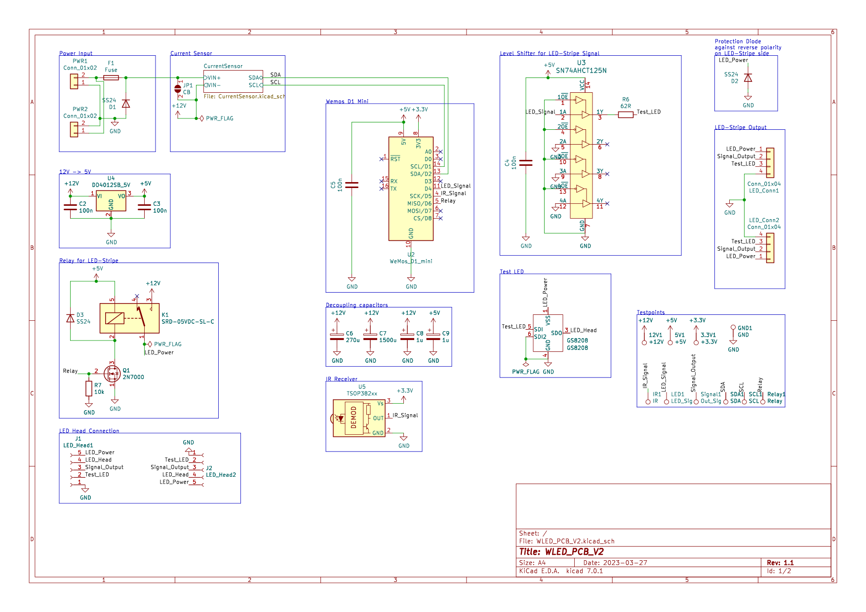
Main components on the WLED PCB V2
WLED PCB V2 bill of materials (BOM)
32 components, 21 distinct parts.
| Qty | Part | Footprint | Refs |
|---|---|---|---|
| 1 | INA219AxD | SOT-23-8_Handsoldering | U1 |
| 1 | WeMos_D1_mini | WEMOS_D1_mini_light | U2 |
| 1 | SN74AHCT125N Texas Instruments | DIP-14_W3mm | U3 |
| 1 | DD4012SB_5V | DD4012S | U4 |
| 1 | TSOP382xx | Vishay_MINICAST-3Pin | U5 |
| 1 | 2N7000 | TO-92_Inline | Q1 |
| 1 | LED_Head1 | PinSocket_1x05_P2.54mm_Vertical | J1 |
| 1 | LED_Head2 | PinSocket_1x05_P2.54mm_Vertical | J2 |
| 1 | Fuse | Fuseholder_Cylinder-5x20mm_Schurter_0031_8201_Horizontal_Open | F1 |
| 1 | GS8208 | GS8208 | GS8208 |
| 1 | SRD-05VDC-SL-C | Relay_SPDT_SANYOU_SRD_Series_Form_C | K1 |
| 2 | Conn_01x04 | JST_XH_S4B-XH-A_1x04_P2.50mm_Horizontal | LED_Conn1, LED_Conn2 |
| 2 | Conn_01x02 | TerminalBlock_bornier-2_P5.08mm | PWR1, PWR2 |
| 3 | SS24 | D_SMB | D1, D2, D3 |
| 5 | 100n | C_0805_2012Metric_Pad1.15x1.40mm_HandSolder | C1, C2, C3, C4, C5 |
| 1 | 270u | C_Radial_D8.0mm_H11.5mm_P3.50mm | C6 |
| 1 | 1500u | C_Radial_D10.0mm_H20.0mm_P5.00mm | C7 |
| 2 | 1u | C_0805_2012Metric_Pad1.15x1.40mm_HandSolder | C8, C9 |
| 3 | 10k | R_0805_2012Metric_Pad1.15x1.40mm_HandSolder | R1, R2, R7 |
| 1 | 0.1R | R_2512_6332Metric_Pad1.52x3.35mm_HandSolder | R3 |
Show 1 more
| Qty | Part | Footprint | Refs |
|---|---|---|---|
| 1 | 62R | R_0805_2012Metric_Pad1.15x1.40mm_HandSolder | R6 |
WLED PCB V2 design files
The KiCad project lives in the jhns-de/WLED-PCB-V2 repository on GitHub; these links point at the commit this page was built from.
WLED PCB V2: common questions
What microcontroller does the WLED PCB V2 use?
The WLED PCB V2 is built around the WeMos_D1_mini, from the ESP8266 family.
How big is the WLED PCB V2?
The WLED PCB V2 measures 95 × 40 mm, has 2 copper layers and is 1.6 mm thick.
How many components are on the WLED PCB V2?
32 components, from 21 distinct parts. The full bill of materials is listed on this page.
Where can I download the WLED PCB V2 design files?
From the jhns-de/WLED-PCB-V2 repository on GitHub, which has the KiCad layout and the schematic; the links under Design files point to each one.
Can I use the WLED PCB V2 design in my own project?
Yes, under the terms of its GPL-3.0 license, which jhns-de chose for the repository.
Can I test firmware for the WLED PCB V2 without the hardware?
Yes. HardLabs builds a simulation of the board from its netlist and BOM, so you can run and debug ESP8266 firmware against it before you order a PCB.
More boards in WLED-PCB-V2
Similar boards
 ESP8266
ESP8266ControllerCircuit
stuartpittaway
75 × 30 mm20 parts2LCC-BY-NC-4.01.1k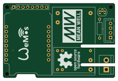 ESP8266
HASwitchPlate
aderusha
60 × 40 mm8 parts2LMIT738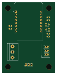 ESP8266
RatGDO-OpenSource-D1Mini-ESP8266
Kaldek
47.8 × 63.3 mm12 parts2LMIT506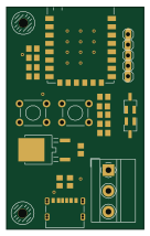 ESP8266
Goatgdo
32.9 × 53.3 mm23 parts2LMIT506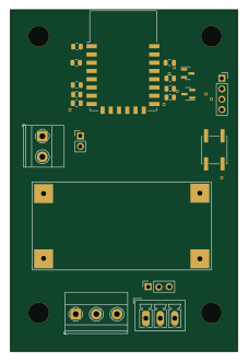 ESP8266
RatGDO-OpenSource-Bare-ESP8266
55 × 82.7 mm20 parts2LMIT506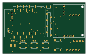 ESP8266
Iaq board
nkitanov
70.1 × 43.2 mm17 parts2LNo license398