
SCAN

About the SCAN PCB
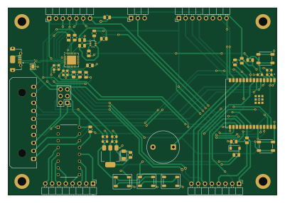
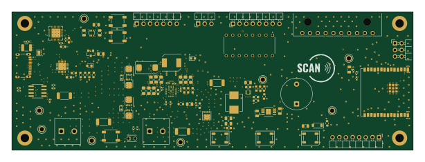
SCAN is an open source ESP32 PCB design by jjsprandel, published on GitHub under the CC-BY-NC-4.0 license. It is a 2-layer board measuring 100 × 70 mm, with 54 components from 38 distinct parts.
Its main chip is the ESP32-C6-WROOM-1-N8, from the ESP32 family. Other key parts include the PCF8574, AMS1117-3.3, TVS2200DRV, ESD122DMYR and CP2102N-A02-xQFN28. By type, the board carries 20 resistors, 11 capacitors, 8 connectors, 6 ICs, 5 diodes and 2 switches.
It belongs with the iot & wireless designs in this gallery.
From the project
Welcome to the SCAN repository! Below, you will find all the necessary information, from hardware design to software documentation.
Welcome to the SCAN repository! Below, you will find all the necessary information, from hardware design to software documentation.
Here are the current statuses of our GitHub workflows:
- CI - Build: Ensures the project builds successfully. - CI - Tests: Runs all unit and integration tests to ensure everything is working as expected. - Docker - Test Build: Attempts Docker Build upon changes to the Dockerfile.

Main components on the SCAN
SCAN bill of materials (BOM)
54 components, 38 distinct parts — part numbers from the project's BOM.
| Qty | Part | Footprint | Refs |
|---|---|---|---|
| 1 | ESP32-C6-WROOM-1-N8 | ESP32-C6-WROOM-1-N8 | U1 |
| 1 | PCF8574 | DIP794W45P254L1969H508Q16 | U2 |
| 1 | AMS1117-3.3 | SOT-223-3_TabPin2 | U3 |
| 1 | TVS2200DRV | WSON-6-1EP_2x2mm_P0.65mm_EP1x1.6mm | U4 |
| 1 | ESD122DMYR | DMY0003A | U5 |
| 1 | CP2102N-A02-xQFN28 | QFN-28-1EP_5x5mm_P0.5mm_EP3.35x3.35mm | U8 |
| 1 | BC847BDW1 | SOT-363_SC-70-6 | Q7 |
| 1 | Conn_01x10 | Molex_Micro-Fit_3.0_43650-1000_1x10_P3.00mm_Horizontal | J1 |
| 1 | KEYPAD_CONN | PinHeader_1x08_P2.54mm_Horizontal | J2 |
| 1 | PN532_CONN | PinHeader_1x08_P2.54mm_Horizontal | J3 |
| 1 | PIR_CONN | PinHeader_1x03_P2.54mm_Horizontal | J4 |
| 1 | DEBUG_BREAKOUT | PinHeader_1x08_P2.54mm_Horizontal | J5 |
| 1 | TFT_CONN | PinHeader_1x07_P2.54mm_Horizontal | J7 |
| 1 | USB_B_Micro | USB_Micro-AB_Molex_47590-0001 | J8 |
| 1 | PWR_MUX | PinHeader_2x03_P2.54mm_Vertical | J11 |
| 1 | Buzzer | Buzzer_12x9.5RM7.6 | BZ1 |
| 1 | RST_SWITCH | SW_SPST_PTS647_Sx38 | SW1 |
| 1 | SW_Push | SW_SPST_PTS647_Sx38 | SW2 |
| 1 | LED | LED_1206_3216Metric | D1 |
| 1 | 1N4148W | D_SOD-123 | D3 |
Show 18 more
| Qty | Part | Footprint | Refs |
|---|---|---|---|
| 1 | SUCCESS_LED | LED_WS2812B_PLCC4_5.0x5.0mm_P3.2mm | D4 |
| 1 | FAILURE_LED | LED_WS2812B_PLCC4_5.0x5.0mm_P3.2mm | D5 |
| 1 | ADMIN_LED | LED_WS2812B_PLCC4_5.0x5.0mm_P3.2mm | D6 |
| 1 | 10u | C_0603_1608Metric | C1 |
| 1 | 0.1u | C_0603_1608Metric | C2 |
| 1 | 1u | C_0603_1608Metric | C3 |
| 2 | 10uF | C_0603_1608Metric | C4, C6 |
| 2 | 100nF | C_0603_1608Metric | C5, C7 |
| 2 | .1u | C_0603_1608Metric | C8, C53 |
| 2 | 4.7u | C_0603_1608Metric | C9, C10 |
| 2 | 2.2k | R_0805_2012Metric | R1, R2 |
| 7 | 10k | R_0805_2012Metric | R3, R4, R5, R6, R10, R34, R37 |
| 1 | 3.3k | R_0805_2012Metric | R7 |
| 1 | 1k | R_0805_2012Metric | R15 |
| 1 | 120 | R_0805_2012Metric | R16 |
| 1 | 47.5k | R_0805_2012Metric | R17 |
| 1 | 22.1k | R_0805_2012Metric | R18 |
| 6 | 0Ω | R_0805_2012Metric | R36, R38, R39, R60, R61, R62 |
SCAN design files
The KiCad project lives in the jjsprandel/SCAN_PCB repository on GitHub; these links point at the commit this page was built from.
SCAN: common questions
What microcontroller does the SCAN use?
The SCAN is built around the ESP32-C6-WROOM-1-N8, from the ESP32 family.
How big is the SCAN PCB?
The SCAN measures 100 × 70 mm, has 2 copper layers and is 1.6 mm thick.
How many components are on the SCAN?
54 components, from 38 distinct parts, with part numbers taken from the project's own BOM. The full bill of materials is listed on this page.
Where can I download the SCAN design files?
From the jjsprandel/SCAN_PCB repository on GitHub, which has the KiCad layout, the schematic and the BOM; the links under Design files point to each one.
Can I use the SCAN design in my own project?
It is published under CC-BY-NC-4.0, which limits how it may be reused; read the license before building on it.
Can I test firmware for the SCAN without the hardware?
Yes. HardLabs builds a simulation of the board from its netlist and BOM, so you can run and debug ESP32 firmware against it before you order a PCB.
More boards in SCAN_PCB
Similar boards
 ESP32
ESP32Open Book Abridged Edition
joeycastillo
85 × 115 mm65 parts2LCC-BY-SA-4.08.1k ESP32
ESP32Badge
atopile
56.3 × 39 mm239 parts4LMIT4.0k ESP32
ESP32Esp32 minimal
36.2 × 26.8 mm20 parts2LMIT4.0k ESP32
ESP32Racer
StuckAtPrototype
36 × 50.2 mm70 parts4LApache-2.03.8k ESP32
ESP32Controller
29 × 74 mm58 parts4LApache-2.03.8k ESP32
ESP32Bitaxe
skot
56.5 × 99.8 mm86 parts4LCERN-OHL-S-2.01.4k