
Gateway node

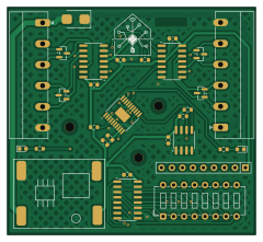
About the Gateway node PCB
Gateway node is an open source WCH CH32/CH55x PCB design by koko69420, published on GitHub. It is a 2-layer board measuring 60 × 55 mm, with 31 components from 18 distinct parts.
Its main chip is the CH32X033F8P6, from the WCH CH32/CH55x family. Other key parts include the 74HC165, MAX491E and AT24C256C-SSHL. By type, the board carries 8 diodes, 7 capacitors, 7 resistors, 6 ICs, 2 connectors and 1 switch.
It belongs with the dev boards & breakouts and iot & wireless designs in this gallery.
From the project
Hard wired home automation, based on a RSICV MCU and RS-422 communication protocol
The HomeBus Gateway Node serves as the vital routing bridge, segmentation barrier, and protocol proxy between the central HomeBus Trunk Backbone Bus and individual Room Sub-Buses.
By dividing the physical automation topology into isolated room-level segments, the Gateway prevents local switch bounces, encoder streams, and internal room traffic from congesting the primary backbone while safeguarding against bus-wide failures.
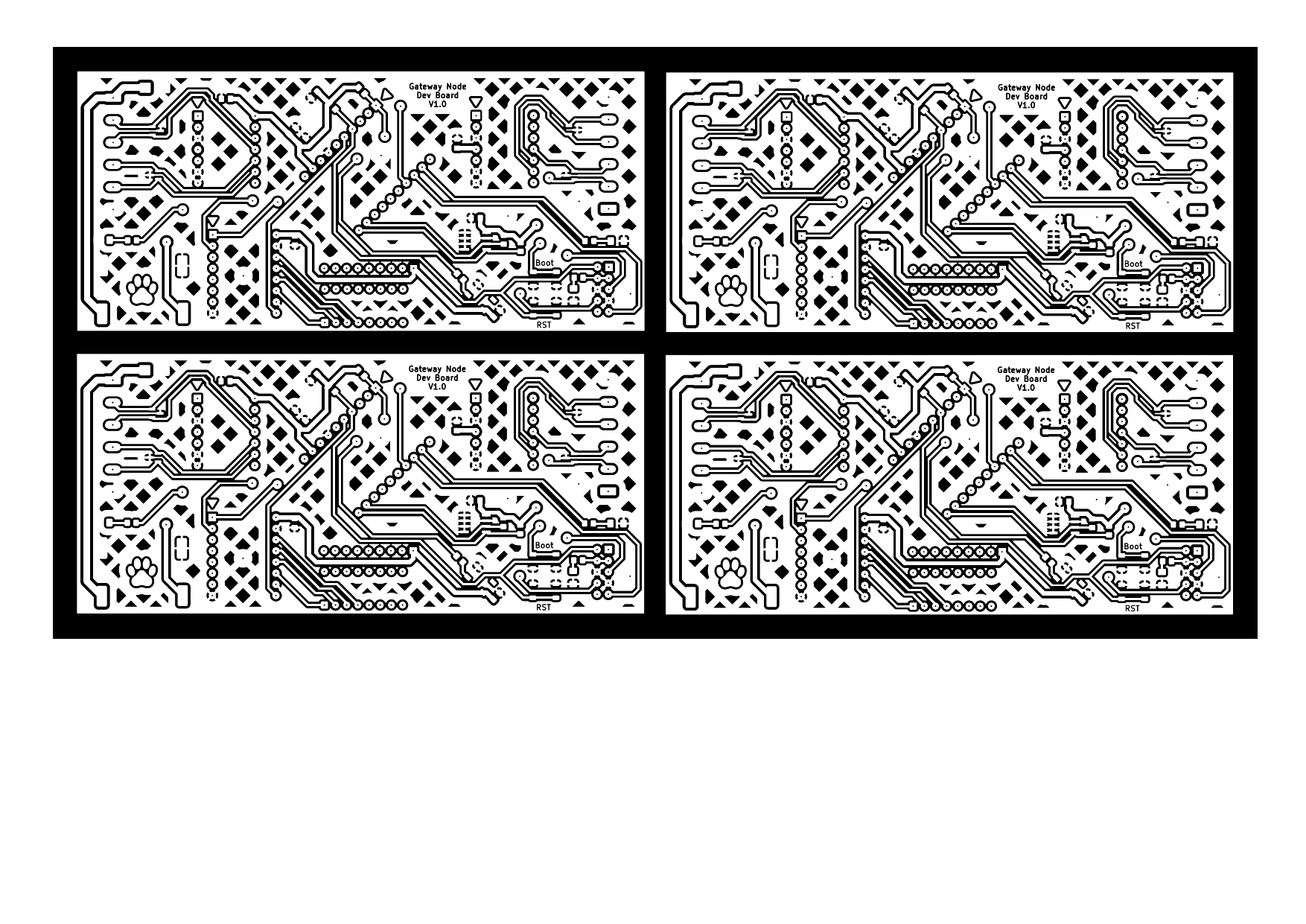
Main components on the Gateway node
Gateway node bill of materials (BOM)
31 components, 18 distinct parts — part numbers from the project's BOM.
| Qty | Part | Footprint | Refs |
|---|---|---|---|
| 1 | CH32X033F8P6 | TSSOP-20-1EP_4.4x6.5mm_P0.65mm_EP2.15x3.35mm | U1 |
| 1 | 74HC165 | SOIC-16_3.9x9.9mm_P1.27mm | U2 |
| 1 | ~ | MP1584 Module | U3 |
| 2 | MAX491E | SOIC-14_3.9x8.7mm_P1.27mm | U4, U5 |
| 1 | AT24C256C-SSHL | SOIC-8_3.9x4.9mm_P1.27mm | U6 |
| 1 | RS-422 Room | PhoenixContact_MC_1,5_6-G-5.08_1x06_P5.08mm_Horizontal | J1 |
| 1 | RS-422 Trunk | PhoenixContact_MC_1,5_6-G-5.08_1x06_P5.08mm_Horizontal | J2 |
| 1 | SW_DIP_x08 | SW_DIP_SPSTx08_Slide_6.7x21.88mm_W7.62mm_P2.54mm_LowProfile | SW1 |
| 1 | D_TVS | D_SMB | D1 |
| 4 | SM712_SOT23 | SOT-23 | D2, D3, D4, D5 |
| 1 | WS2812B | XINGLIGHT-XL-1010RGBC-WS2812B | D6 |
| 2 | LED | LED_0603_1608Metric | D7, D8 |
| 6 | 100nF | C_0603_1608Metric | C1, C2, C4, C5, C6, C7 |
| 1 | 10uF | C_0603_1608Metric | C3 |
| 1 | 330Ω | R_0603_1608Metric | R1 |
| 3 | 10KΩ | R_0603_1608Metric | R2, R3, R4 |
| 2 | 4.7kΩ | R_0603_1608Metric | R5, R6 |
| 1 | 10KΩ | R_Array_SIP9 | RN1 |
Gateway node design files
The KiCad project lives in the koko69420/HomeBus repository on GitHub; these links point at the commit this page was built from.
Gateway node: common questions
What microcontroller does the Gateway node use?
The Gateway node is built around the CH32X033F8P6, from the WCH CH32/CH55x family.
How big is the Gateway node PCB?
The Gateway node measures 60 × 55 mm, has 2 copper layers and is 1.6 mm thick.
How many components are on the Gateway node?
31 components, from 18 distinct parts, with part numbers taken from the project's own BOM. The full bill of materials is listed on this page.
Where can I download the Gateway node design files?
From the koko69420/HomeBus repository on GitHub, which has the KiCad layout, the schematic and the BOM; the links under Design files point to each one.
Can I use the Gateway node design in my own project?
The repository has no license, so all rights stay with koko69420. Use it as a reference, and ask the author before reusing the design.
Can I test firmware for the Gateway node without the hardware?
Yes. HardLabs builds a simulation of the board from its netlist and BOM, so you can run and debug WCH CH32/CH55x firmware against it before you order a PCB.
More boards in HomeBus
 WCH CH32/CH55x
Fan Controller node
100 × 100 mm51 parts2LNo license0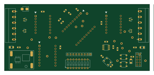 WCH CH32/CH55x
HomeBus Gateway Node Development Board
130 × 60 mm38 parts2LNo license0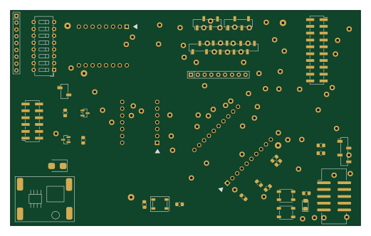 WCH CH32/CH55x
Base Node Test Board
130 × 80 mm36 parts2LNo license0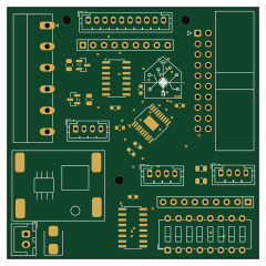 WCH CH32/CH55x
Base node
60 × 60 mm29 parts2LNo license0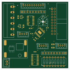 WCH CH32/CH55x
Base node rounded
60 × 60 mm27 parts2LNo license0 WCH CH32/CH55x
Expanders
21.1 × 26.8 mm9 parts2LNo license0
Similar boards
 WCH CH32/CH55x
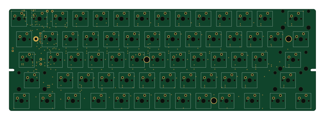
CH32X-60-ANSI-Improved
rgoulter
285 × 94.2 mm149 parts2LNo license230 WCH CH32/CH55x
CH552-48
224.6 × 74.2 mm107 parts2LNo license230 WCH CH32/CH55x
CH32X-48
224.6 × 74.2 mm112 parts2LNo license230 WCH CH32/CH55x
CH32X-75
285 × 94.2 mm318 parts2LNo license230 WCH CH32/CH55x
Idawgz32
ChrisChrisLoLo
98.7 × 45.5 mm81 parts2LGPL-3.077 WCH CH32/CH55x
Pointify
luftaquila
23.1 × 20.7 mm8 parts2LGPL-3.042