
Aesa test

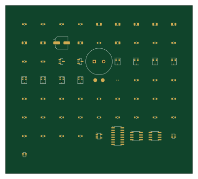
About the Aesa test PCB
Aesa test is an open source PCB design by tieziyun, published on GitHub. It is a 2-layer board measuring 100 × 90 mm, with 62 components from 22 distinct parts.
Other key parts include the 74AHCT1G125, 74AHCT595D, UCC27524DR, OPA1678IDR and 74LVC2G34. By type, the board carries 25 resistors, 20 capacitors, 8 microphones, 6 ICs, 2 diodes and 1 speaker.
It belongs with the power & battery designs in this gallery.
From the project
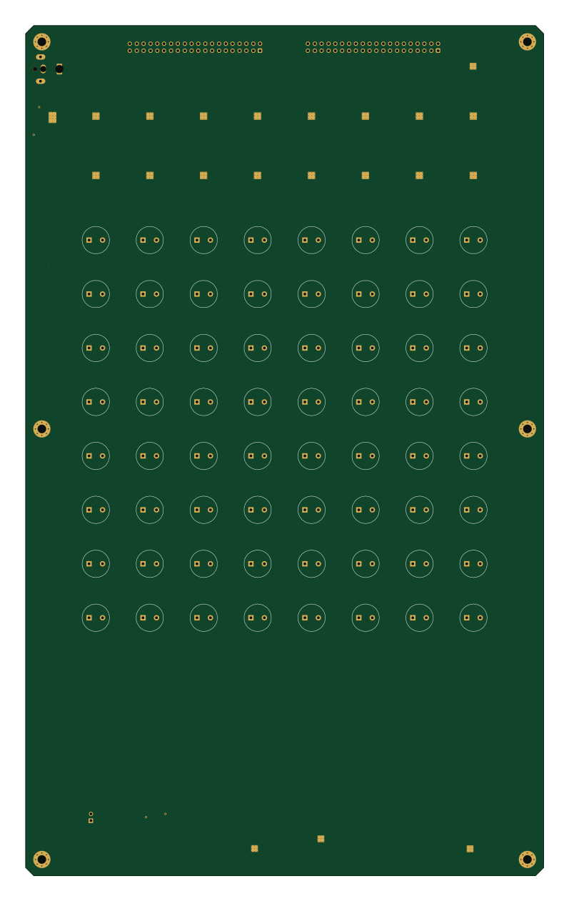
A 40 kHz in-air phased array, an acoustic "AESA". It has 64 transducers in an 8 × 8 grid, and each one can transmit or listen under FPGA control, element by element and ping by ping. Eight wideband MEMS microphones sit around the edge of the grid. Every element's raw waveform (am
A 40 kHz in-air phased array, an acoustic "AESA". It has 64 transducers in an 8 × 8 grid, and each one can transmit or listen under FPGA control, element by element and ping by ping. Eight wideband MEMS microphones sit around the edge of the grid. Every element's raw waveform (amplitude and phase) is digitised and streamed to an ALINX AXU3EGB (Zynq UltraScale+ ZU3EG) board, which does the beamforming.
Main components on the Aesa test
Aesa test bill of materials (BOM)
62 components, 22 distinct parts — part numbers from the project's BOM.
| Qty | Part | Footprint | Refs |
|---|---|---|---|
| 1 | 74AHCT1G125 | SOT-23-5 | U1 |
| 1 | 74AHCT595D | SOIC-16_3.9x9.9mm_P1.27mm | U2 |
| 1 | UCC27524DR | SOIC-8_3.9x4.9mm_P1.27mm | U3 |
| 1 | OPA1678IDR | SOIC-8_3.9x4.9mm_P1.27mm | U4 |
| 2 | 74LVC2G34 | SOT-363_SC-70-6 | U5, U6 |
| 1 | CUSA-TR65-065-2200-TH68 | CUSA-TR65 | LS1 |
| 8 | SPH0641LU4H-1 | Knowles_LGA-5_3.5x2.65mm | MK1, MK2, MK3, MK4, MK5, MK6, MK7, MK8 |
| 2 | BAV99 | SOT-23 | D1, D2 |
| 7 | 100n 16V X7R | C_0603_1608Metric | C1, C3, C6, C7, C8, C11, C12 |
| 1 | 47u 35V | CP_Elec_6.3x7.7 | C2 |
| 1 | 1u 50V X7R | C_0805_2012Metric | C4 |
| 1 | 100n 50V X7R | C_0603_1608Metric | C5 |
| 2 | 1n 50V C0G 1% | C_0603_1608Metric | C9, C10 |
| 8 | 100n 16V C0G | C_0805_2012Metric | C13, C14, C15, C16, C17, C18, C19, C20 |
| 4 | 10k 1% | R_0603_1608Metric | R1, R2, R3, R7 |
| 1 | 47 1% | R_0603_1608Metric | R4 |
| 2 | 100k 1% | R_0603_1608Metric | R5, R13 |
| 1 | 4.7k 1% | R_0603_1608Metric | R6 |
| 3 | 2k 1% | R_0603_1608Metric | R8, R9, R10 |
| 1 | 16k 1% | R_0603_1608Metric | R11 |
Show 2 more
| Qty | Part | Footprint | Refs |
|---|---|---|---|
| 1 | 100 1% | R_0603_1608Metric | R12 |
| 12 | 33 1% | R_0603_1608Metric | R14, R15, R16, R17, R18, R19, R20, R21 +4 |
Aesa test design files
The KiCad project lives in the tieziyun/ultrasonic-aesa repository on GitHub; these links point at the commit this page was built from.
Aesa test: common questions
How big is the Aesa test PCB?
The Aesa test measures 100 × 90 mm, has 2 copper layers and is 1.6 mm thick.
How many components are on the Aesa test?
62 components, from 22 distinct parts, with part numbers taken from the project's own BOM. The full bill of materials is listed on this page.
Where can I download the Aesa test design files?
From the tieziyun/ultrasonic-aesa repository on GitHub, which has the KiCad layout and the BOM; the links under Design files point to each one.
Can I use the Aesa test design in my own project?
The repository has no license, so all rights stay with tieziyun. Use it as a reference, and ask the author before reusing the design.
More boards in ultrasonic-aesa
Similar boards
EinkPDA screen
TalismanDesign
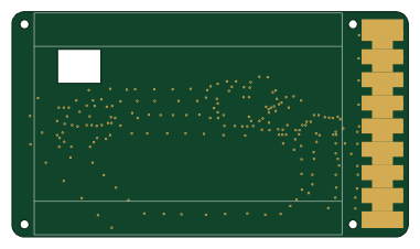
95 × 54 mm27 parts2LApache-2.02.0k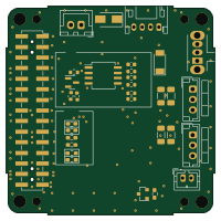
Stack chan
stack-chan
50 × 50 mm33 parts2LApache-2.01.7k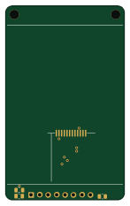
Display Carrier
AxxAxx
35.6 × 58.2 mm5 parts2LGPL-3.01.7k
ProgrammingAdapter
stuartpittaway
10.5 × 83 mm3 parts2LCC-BY-NC-4.01.1k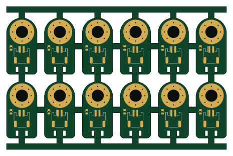
TemperaturePCB PANEL
116 × 75.5 mm178 parts2LCC-BY-NC-4.01.1k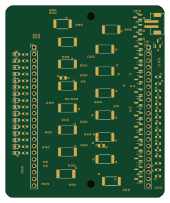
Module 16S PassiveBalanceAddOn
61 × 74 mm86 parts2LCC-BY-NC-4.01.1k