
169 node

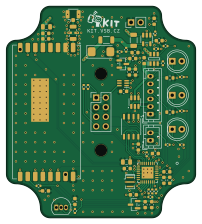
About the 169 node PCB
169 node is an open source AVR/Arduino PCB design by vsb-fei-440, published on GitHub under the MIT license. It is a 4-layer board measuring 50 × 55.9 mm, with 65 components from 33 distinct parts.
Its main chip is the ATMEGA328P-M, from the AVR/Arduino family. Other key parts include the TPS2553DDBVR, TPS22919DCKR, USBLC6-2SC6, INA180A2 and DS18B20. By type, the board carries 23 capacitors, 20 resistors, 10 ICs, 5 connectors, 3 diodes and 2 inductors.
It belongs with the rf & radio and usb & debug tools designs in this gallery.
From the project
A complete LoRa system for the 169 MHz band (169.4375 MHz): battery-powered nodes, a gateway board, a Raspberry Pi bridge to MQTT and Grafana dashboards. It was built at VSB - Technical University of Ostrava for teaching and for coverage measurements of the 169 MHz band.
A complete LoRa system for the 169 MHz band (169.4375 MHz): battery-powered nodes, a gateway board, a Raspberry Pi bridge to MQTT and Grafana dashboards. It was built at VSB - Technical University of Ostrava for teaching and for coverage measurements of the 169 MHz band.
1. A node measures on a button press: it sends three short frames with its ID, a measurement number, its transmit power, battery voltage and temperature. 2. The gateway receives the frame, the Raspberry Pi checks it and immediately sends an acknowledgement (ACK) carrying the signal strength the gateway measured. 3. The node…
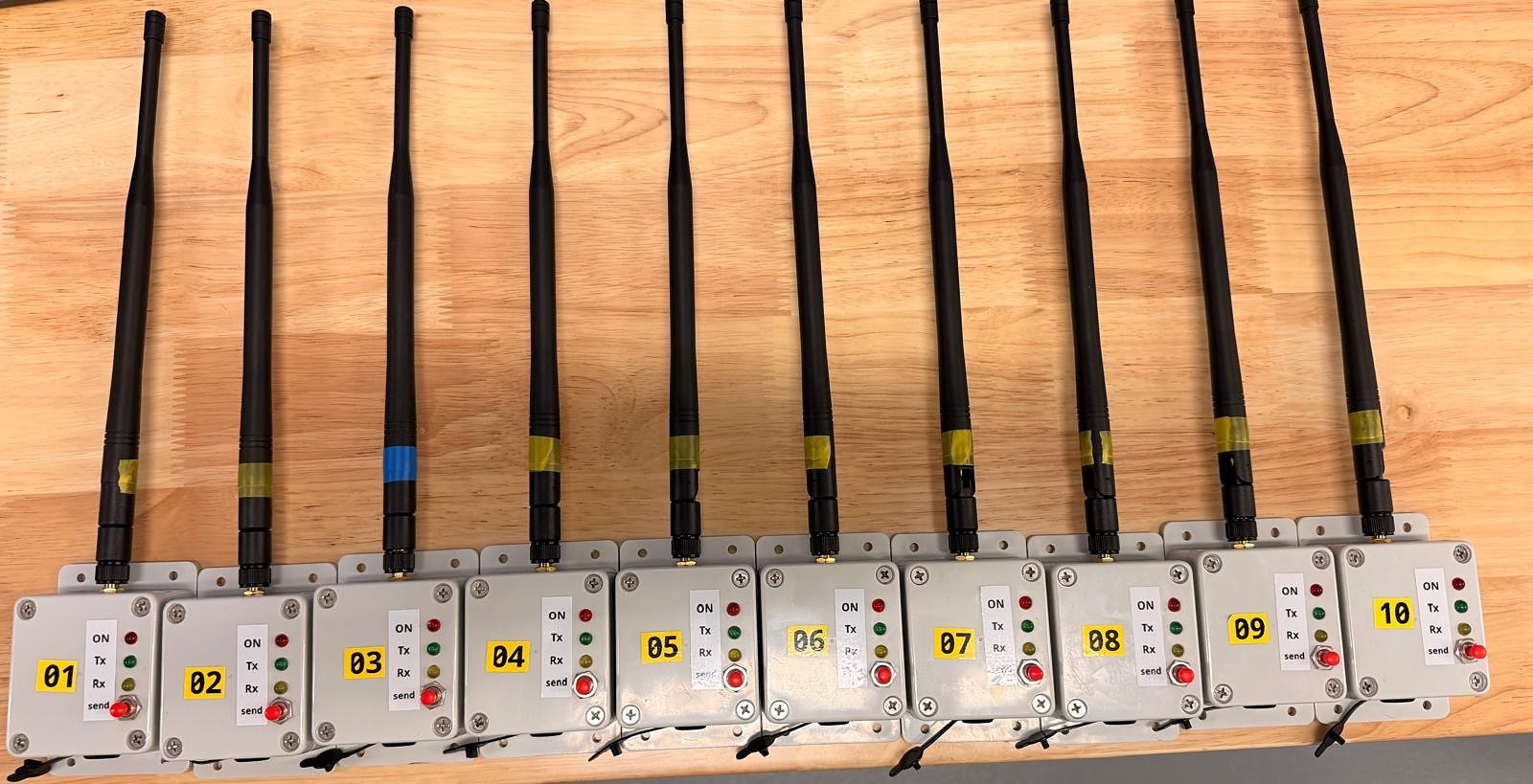
Main components on the 169 node
169 node bill of materials (BOM)
65 components, 33 distinct parts — part numbers from the project's BOM.
| Qty | Part | Footprint | Refs |
|---|---|---|---|
| 1 | TPS2553DDBVR TPS2553DDBVR_EDIT | SOT95P280X145-6N | IC1 |
| 1 | TPS22919DCKR | SOT65P210X110-6N | IC2 |
| 1 | USBLC6-2SC6 | SOT-23-6 | U1 |
| 1 | ATMEGA328P-M ATmega328P-M | QFN-32-1EP_5x5mm_P0.5mm_EP3.1x3.1mm | U2 |
| 1 | INA180A2 | SOT-23-5 | U3 |
| 1 | DS18B20 | TO-92_Inline | U4 |
| 2 | MCP1700X-330XXTT MCP1700x-330xxTT | SOT-23 | U5, U7 |
| 1 | RFM98PW-169S2 | XCVR_RFM98PW-169S2_EDIT | U6 |
| 1 | CH340N | JEITA_SOIC-8_3.9x4.9mm_P1.27mm | U8 |
| 1 | C341524 Resonator | Resonator_SMD_Murata_CSTxExxV-3Pin_3.0x1.1mm | Y1 |
| 1 | C131342 USB-C | JST_PH_B6B-PH-K_1x06_P2.00mm_Vertical | J1 |
| 1 | C131337 TX_BTN | JST_PH_B2B-PH-K_1x02_P2.00mm_Vertical | J2 |
| 1 | C492401 I_RAW | PinHeader_1x02_P2.54mm_Vertical | J3 |
| 1 | CONN_02X04_COUNTER_CLOCKWISE Conn_02x04_Counter_Clockwise | PinHeader_2x04_P2.54mm_Vertical | J4 |
| 1 | C47986640 Conn_Coaxial | U.FL_Hirose_U.FL-R-SMT-1_Vertical | J5 |
| 1 | LFCN-190 | Filter_Mini-Circuits_FV1206 | FL1 |
| 1 | POWER_RED | LED_D5.0mm | D1 |
| 1 | TX_GREEN | LED_D5.0mm | D2 |
| 1 | RX_GREEN | LED_D5.0mm | D3 |
| 1 | C527608 FerriteBead | L_1206_3216Metric | FB1 |
Show 13 more
| Qty | Part | Footprint | Refs |
|---|---|---|---|
| 1 | 10U 10u | L_0603_1608Metric | L1 |
| 14 | 100N 100n | C_0603_1608Metric | C1, C2, C3, C5, C6, C7, C8, C11 +6 |
| 2 | 10U 10u | C_0805_2012Metric | C4, C20 |
| 6 | 1u | C_0603_1608Metric | C9, C10, C12, C13, C14, C19 |
| 1 | 100U 100u | CP_EIA-6032-28_Kemet-C | C21 |
| 6 | 100K 100k | R_0402_1005Metric | R1, R7, R9, R10, R11, R16 |
| 1 | 20K 20k | R_0402_1005Metric | R2 |
| 4 | 22 | R_0402_1005Metric | R3, R4, R5, R20 |
| 1 | 10K 10k | R_0402_1005Metric | R6 |
| 1 | 0R1 | R_1206_3216Metric | R8 |
| 1 | 1k | C_0402_1005Metric | R12 |
| 3 | 4K7 4k7 | R_0402_1005Metric | R15, R21, R22 |
| 3 | 100 | C_0402_1005Metric | R17, R18, R19 |
169 node design files
The KiCad project lives in the vsb-fei-440/LoRa-169 repository on GitHub; these links point at the commit this page was built from.
169 node: common questions
What microcontroller does the 169 node use?
The 169 node is built around the ATMEGA328P-M, from the AVR/Arduino family.
How big is the 169 node PCB?
The 169 node measures 50 × 55.9 mm, has 4 copper layers and is 1.6062 mm thick.
How many components are on the 169 node?
65 components, from 33 distinct parts, with part numbers taken from the project's own BOM. The full bill of materials is listed on this page.
Where can I download the 169 node design files?
From the vsb-fei-440/LoRa-169 repository on GitHub, which has the KiCad layout, the schematic and the BOM; the links under Design files point to each one.
Can I use the 169 node design in my own project?
Yes, under the terms of its MIT license, which vsb-fei-440 chose for the repository.
Can I test firmware for the 169 node without the hardware?
Yes. HardLabs builds a simulation of the board from its netlist and BOM, so you can run and debug AVR/Arduino firmware against it before you order a PCB.
More boards in LoRa-169
Similar boards
 AVR/Arduino
Magspoof
samyk
35 × 29 mm11 parts2LNo license4.2k AVR/Arduino
Redox keyboard
mattdibi
162.2 × 126.5 mm77 parts2LMIT2.0k AVR/Arduino
Labrador
espotek-org
36.8 × 34.7 mm75 parts2LNo license1.2k AVR/Arduino
ModuleV450
stuartpittaway
30 × 61.4 mm39 parts2LCC-BY-NC-4.01.1k AVR/Arduino
V4
30 × 50 mm38 parts2LCC-BY-NC-4.01.1k AVR/Arduino
Discipline
coseyfannitutti
304.9 × 122.8 mm170 parts2LCC-BY-NC-4.01.0k