
Synchronisation-Wand

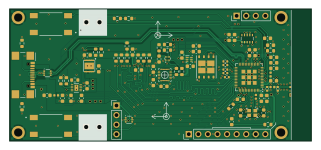
About the Synchronisation-Wand PCB
Synchronisation-Wand is an open source ESP32 PCB design by YuxuanHan0326, published on GitHub under the Apache-2.0 license. It is a 4-layer board measuring 80 × 35 mm, with 90 components from 40 distinct parts.
Its main chip is the ESP32-S3, from the ESP32 family. Other key parts include the USBLC6-2P6, BQ25185DLHR, NCV59801CML330TCG, TLV70018DSER and ICM-20948. By type, the board carries 35 capacitors, 34 resistors, 10 ICs, 5 connectors, 4 inductors and 2 crystals.
It belongs with the sensors, iot & wireless and wearables designs in this gallery.
From the project
Hardware for synchronising wearables using magnetometers
The related publication focuses mainly on the Synchronisation Wand device and hardware design. The final report is complementary and covers the verification platform, encoded EMP synchronisation verification, data processing workflow, and analysis in more detail. The presentation poster is a concise visual summary of the verification work.
The device includes an OLED display and 4 configuable push buttons for user interface to enhance the usability of the system. The device uses SD card as storage medium to store the synchronising data and onboard IMU data. WiFi is used to synchronise the…
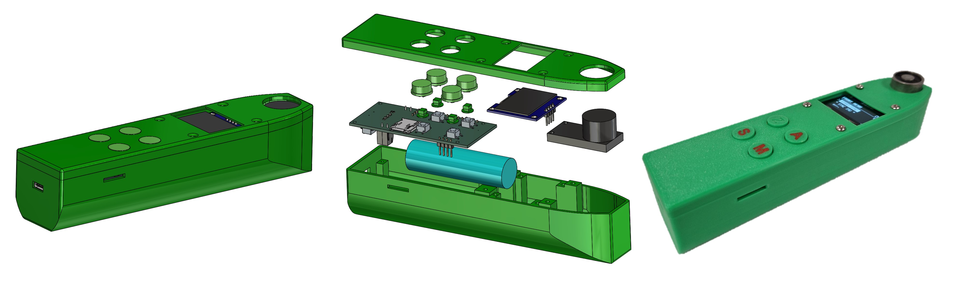
Main components on the Synchronisation-Wand
Synchronisation-Wand bill of materials (BOM)
90 components, 40 distinct parts — part numbers from the project's BOM.
| Qty | Part | Footprint | Refs |
|---|---|---|---|
| 2 | USBLC6-2P6 | SOT-666 | U1, U2 |
| 1 | BQ25185DLHR | WSON10_DLH_TEX | U3 |
| 1 | NCV59801CML330TCG | SON65P300X300X100-9N-D | U4 |
| 1 | TLV70018DSER | DSE0006A | U5 |
| 1 | ICM-20948 | QFN24_3X3X0P9_IVS | U6 |
| 1 | ESP32-S3 | QFN-56-1EP_7x7mm_P0.4mm_EP4x4mm | U7 |
| 1 | PCA9306DQER | PCA9306DQER | U8 |
| 1 | PUSB3FR6Z | PUSB3FR6Z | U9 |
| 1 | GD25Q256EWIGR | WSON-8-1EP_6x5mm_P1.27mm_EP3.4x4.3mm | U10 |
| 1 | 830108208709 | 830108208709 | Y1 |
| 1 | TG-3541CE 32.7680KXA3 TG-3541CE_32.7680KXA3 | TG3541CE327680KXA3 | Y2 |
| 1 | USB4110-GF-A | USB4110-GF-A_GCT | J1 |
| 2 | CONN_01X04_PIN Conn_01x04_Pin | PinHeader_1x04_P2.54mm_Vertical | J2, J6 |
| 1 | CONN_01X09_PIN Conn_01x09_Pin | PinHeader_1x09_P2.54mm_Vertical | J4 |
| 1 | DM3AT-SF-PEJM540 | CONN8_DM3AT-SF-PEJM5_HIR | J5 |
| 1 | 2.2NH 2.2nH | L_0402_1005Metric | L1 |
| 1 | 24NH 24nH | L_0402_1005Metric | L2 |
| 1 | 2.7NH 2.7nH | L_0402_1005Metric | L3 |
| 1 | 2NH 2nH | L_0402_1005Metric | L4 |
| 15 | 0.1UF 0.1uF | C_0603_1608Metric | C1, C2, C7, C11, C12, C13, C16, C17 +7 |
Show 20 more
| Qty | Part | Footprint | Refs |
|---|---|---|---|
| 9 | 1UF 1uF | C_0603_1608Metric | C3, C5, C6, C9, C14, C20, C25, C29 +1 |
| 5 | 10UF 10uF | C_0603_1608Metric | C4, C8, C10, C26, C35 |
| 1 | 18PF 18pF | C_0603_1608Metric | C15 |
| 1 | 0.01UF 0.01uF | C_0603_1608Metric | C19 |
| 2 | 1.8PF 1.8pF | C_0402_1005Metric | C21, C22 |
| 2 | 10PF 10pF | C_0603_1608Metric | C27, C30 |
| 3 | 5K1 | R_0603_1608Metric | R1, R2, R34 |
| 10 | 10K | R_0603_1608Metric | R3, R4, R7, R24, R25, R26, R27, R28 +2 |
| 2 | 100K | R_0603_1608Metric | R5, R6 |
| 1 | 560 | R_0603_1608Metric | R8 |
| 1 | 18K | R_0603_1608Metric | R9 |
| 1 | 33K | R_0603_1608Metric | R10 |
| 1 | 82K | R_0603_1608Metric | R11 |
| 1 | 1K5 | R_0603_1608Metric | R12 |
| 4 | 3K3 | R_0603_1608Metric | R15, R16, R31, R33 |
| 5 | 0 | R_0402_1005Metric | R17, R18, R19, R20, R21 |
| 1 | 499 | R_0603_1608Metric | R22 |
| 1 | 200K | R_0603_1608Metric | R23 |
| 2 | 1K | R_0603_1608Metric | R30, R32 |
| 1 | 470 | R_0603_1608Metric | R36 |
Synchronisation-Wand design files
The KiCad project lives in the YuxuanHan0326/Synchronisation-Wand repository on GitHub; these links point at the commit this page was built from.
Synchronisation-Wand: common questions
What microcontroller does the Synchronisation-Wand use?
The Synchronisation-Wand is built around the ESP32-S3, from the ESP32 family.
How big is the Synchronisation-Wand PCB?
The Synchronisation-Wand measures 80 × 35 mm, has 4 copper layers and is 1.6162 mm thick.
How many components are on the Synchronisation-Wand?
90 components, from 40 distinct parts, with part numbers taken from the project's own BOM. The full bill of materials is listed on this page.
Where can I download the Synchronisation-Wand design files?
From the YuxuanHan0326/Synchronisation-Wand repository on GitHub, which has the KiCad layout, the schematic and the BOM; the links under Design files point to each one.
Can I use the Synchronisation-Wand design in my own project?
Yes, under the terms of its Apache-2.0 license, which YuxuanHan0326 chose for the repository.
Can I test firmware for the Synchronisation-Wand without the hardware?
Yes. HardLabs builds a simulation of the board from its netlist and BOM, so you can run and debug ESP32 firmware against it before you order a PCB.
Similar boards
 ESP32
ESP32Open Book Abridged Edition
joeycastillo
85 × 115 mm65 parts2LCC-BY-SA-4.08.1k ESP32
ESP32Badge
atopile
56.3 × 39 mm239 parts4LMIT4.0k ESP32
ESP32Esp32 minimal
36.2 × 26.8 mm20 parts2LMIT4.0k ESP32
ESP32Racer
StuckAtPrototype
36 × 50.2 mm70 parts4LApache-2.03.8k ESP32
ESP32Controller
29 × 74 mm58 parts4LApache-2.03.8k ESP32
ESP32Bitaxe
skot
56.5 × 99.8 mm86 parts4LCERN-OHL-S-2.01.4k