
Project A

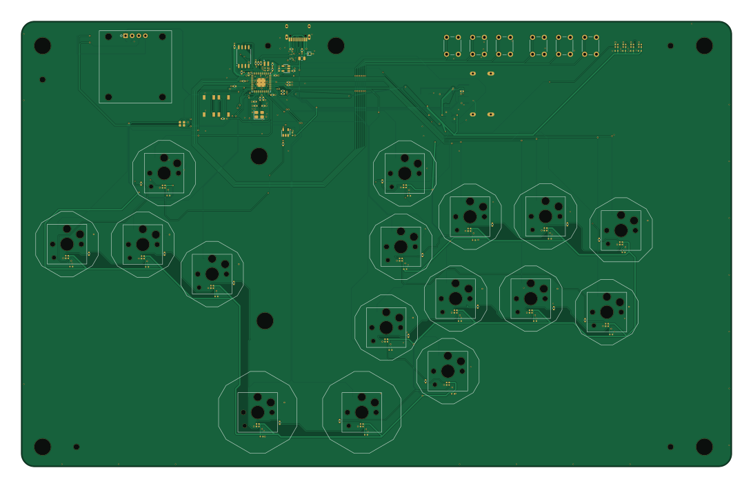
About the Project A PCB
Project A is an open source RP2040/RP2350 PCB design by zephris, published on GitHub under the GPL-2.0 license. It is a 4-layer board measuring 272.6 × 171 mm, with 112 components from 35 distinct parts.
Its main chip is the RP2350_60QFN, from the RP2040/RP2350 family. Other key parts include the TLV73333PDBV, W25Q128JVS, ECMF2-40A100N6, WEA012864DWPP3N00003 and SN74LV1T34DBVR. By type, the board carries 44 capacitors, 32 resistors, 21 diodes, 8 ICs, 2 switches and 1 crystal.
It belongs with the keyboards designs in this gallery.
From the project
fresh CAD for first hitbox
Latest copper/via cleanup and focused JLCPCB checks: review and recovery record.
Use the root Flatbox-rev8.kicadpro`. The accepted PCB has four copper layers with two dedicated inner GND planes. The 2026-10-03 main-project merge passes ERC, DRC and schematic parity with zero findings and zero open connections. Validation evidence, recovery backup and remaining release checks are in the merge record. Eight unnecessary routing bridges were subsequently simplified, removing 16 vias; the bridge record contains the latest verification and PCB backup.
Main components on the Project A
Project A bill of materials (BOM)
112 components, 35 distinct parts — part numbers from the project's BOM.
| Qty | Part | Footprint | Refs |
|---|---|---|---|
| 1 | RP2350_60QFN | RP2350-QFN-60-1EP_7x7_P0.4mm_EP3.4x3.4mm_ThermalVias | U1 |
| 1 | TLV73333PDBV | SOT-23-5 | U2 |
| 1 | W25Q128JVS | SOIC-8_5.23x5.23mm_P1.27mm | U3 |
| 1 | ECMF2-40A100N6 STMicroelectronics | ECMF2-40A100N6 | U4 |
| 1 | WEA012864DWPP3N00003 Winstar | OLED_WEA012864DWPP3N00003 | U5 |
| 1 | SN74LV1T34DBVR Texas Instruments | SOT-23-5 | U6 |
| 1 | TPS2553DBVR Texas Instruments | SOT-23-6 | U7 |
| 1 | USBLC6-2SC6 STMicroelectronics | SOT-23-6 | U8 |
| 1 | ABM8-272-T3 | Crystal_SMD_3225-4Pin_3.2x2.5mm | Y1 |
| 1 | SMD0805-075-12V 750mA hold TECHFUSE | Fuse_0805_2012Metric | F1 |
| 2 | SW_Push | SW_C318884_FabOnly | SW19, SW20 |
| 1 | HRO-TYPE-C-31-M-12 | HRO-TYPE-C-31-M-12-Assembly | USB1 |
| 1 | C2763302 USB_A | C2763302 | USB2 |
| 20 | SK6805-EC15 OPSCO | LED_SK6805_EC15_Optical | D1, D2, D3, D4, D5, D6, D7, D8 +12 |
| 1 | ESDA7P120-1U1M STMicroelectronics | ST_QFN-2L_1.6x1.0mm | D21 |
| 1 | 3.3U 3.3u | L_pol_2016 | L1 |
| 10 | 100N 100n | C_0402_1005Metric | C1, C3, C4, C5, C6, C7, C8, C9 +2 |
| 2 | 4.7U 4.7u | C_0402_1005Metric | C2, C11 |
| 2 | 4.7U 4.7u | C_0402_1005Metric_small_pads | C12, C13 |
| 2 | 1u | C_0402_1005Metric | C14, C15 |
Show 15 more
| Qty | Part | Footprint | Refs |
|---|---|---|---|
| 2 | 15P 15p | C_0402_1005Metric | C16, C17 |
| 2 | T520B107M010ATE070 100u/10V KEMET | CP_KEMET_T520B_3528_21 | C19, C43 |
| 21 | CL05B104KO5NNNC 100n Samsung Electro-Mechanics | C_0402_1005Metric_small_pads | C20, C21, C22, C23, C24, C25, C26, C27 +13 |
| 1 | 1u/10V/X7R | C_0603_1608Metric | C41 |
| 2 | CL05B104KO5NNNC 100n Samsung Electro-Mechanics | C_0402_1005Metric | C42, C44 |
| 1 | 33 | R_0402_1005Metric | R1 |
| 2 | 27 | R_0402_1005Metric | R2, R3 |
| 3 | 1k | R_0402_1005Metric | R4, R6, R8 |
| 2 | 22 | R_0402_1005Metric | R5, R7 |
| 2 | 5.1K 5.1k | R_0402_1005Metric | R10, R11 |
| 2 | 0603WAF4701T5E 4.7k UNI-ROYAL | R_0603_Compact | R12, R13 |
| 1 | 0402WGF5100TCE 510R UNI-ROYAL | R_0402_1005Metric | R14 |
| 1 | 0402WGF2003TCE 200k 1% UNI-ROYAL | R_0402_1005Metric | R15 |
| 2 | 0402WGF1002TCE 10k UNI-ROYAL | R_0402_1005Metric | R16, R17 |
| 16 | 0402WGF1000TCE 100R UNI-ROYAL | R_0402_1005Metric | R18, R19, R20, R21, R22, R23, R24, R25 +8 |
Project A design files
The KiCad project lives in the zephris/project_A repository on GitHub; these links point at the commit this page was built from.
- LayoutFlatbox-rev8.kicad_pcb
- SchematicFlatbox-rev8.kicad_sch
- BOMproduction/bom.csv
Project A: common questions
What microcontroller does the Project A use?
The Project A is built around the RP2350_60QFN, from the RP2040/RP2350 family.
How big is the Project A PCB?
The Project A measures 272.6 × 171 mm, has 4 copper layers and is 1.6 mm thick.
How many components are on the Project A?
112 components, from 35 distinct parts, with part numbers taken from the project's own BOM. The full bill of materials is listed on this page.
Where can I download the Project A design files?
From the zephris/project_A repository on GitHub, which has the KiCad layout, the schematic and the BOM; the links under Design files point to each one.
Can I use the Project A design in my own project?
Yes, under the terms of its GPL-2.0 license, which zephris chose for the repository.
Can I test firmware for the Project A without the hardware?
Yes. HardLabs builds a simulation of the board from its netlist and BOM, so you can run and debug RP2040/RP2350 firmware against it before you order a PCB.
Similar boards
 RP2040/RP2350
OSO-BOOK-C1
joeycastillo
85 × 115 mm29 parts2LCC-BY-SA-4.08.1k RP2040/RP2350
Corne chocolate
foostan
277.2 × 107.5 mm164 parts2LCC-BY-4.07.7k RP2040/RP2350
Corne cherry
277.2 × 107.5 mm164 parts2LCC-BY-4.07.7k RP2040/RP2350
Jitx design
gusmanb
55.5 × 65 mm26 parts4LGPL-3.05.0k RP2040/RP2350
LogicAnalyzer
57 × 55.2 mm6 parts2LGPL-3.05.0k RP2040/RP2350
Main
google
98 × 71 mm102 parts2LApache-2.02.9k