
Flat contact test


About the Flat contact test PCB
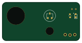
Flat contact test is an open source PCB design by Bruhdows, published on GitHub. It is a 2-layer board measuring 20 × 12 mm, with 6 components from 6 distinct parts.
By type, the board carries 5 test points and 1 connector.
It belongs with the sensors designs in this gallery.
From the project
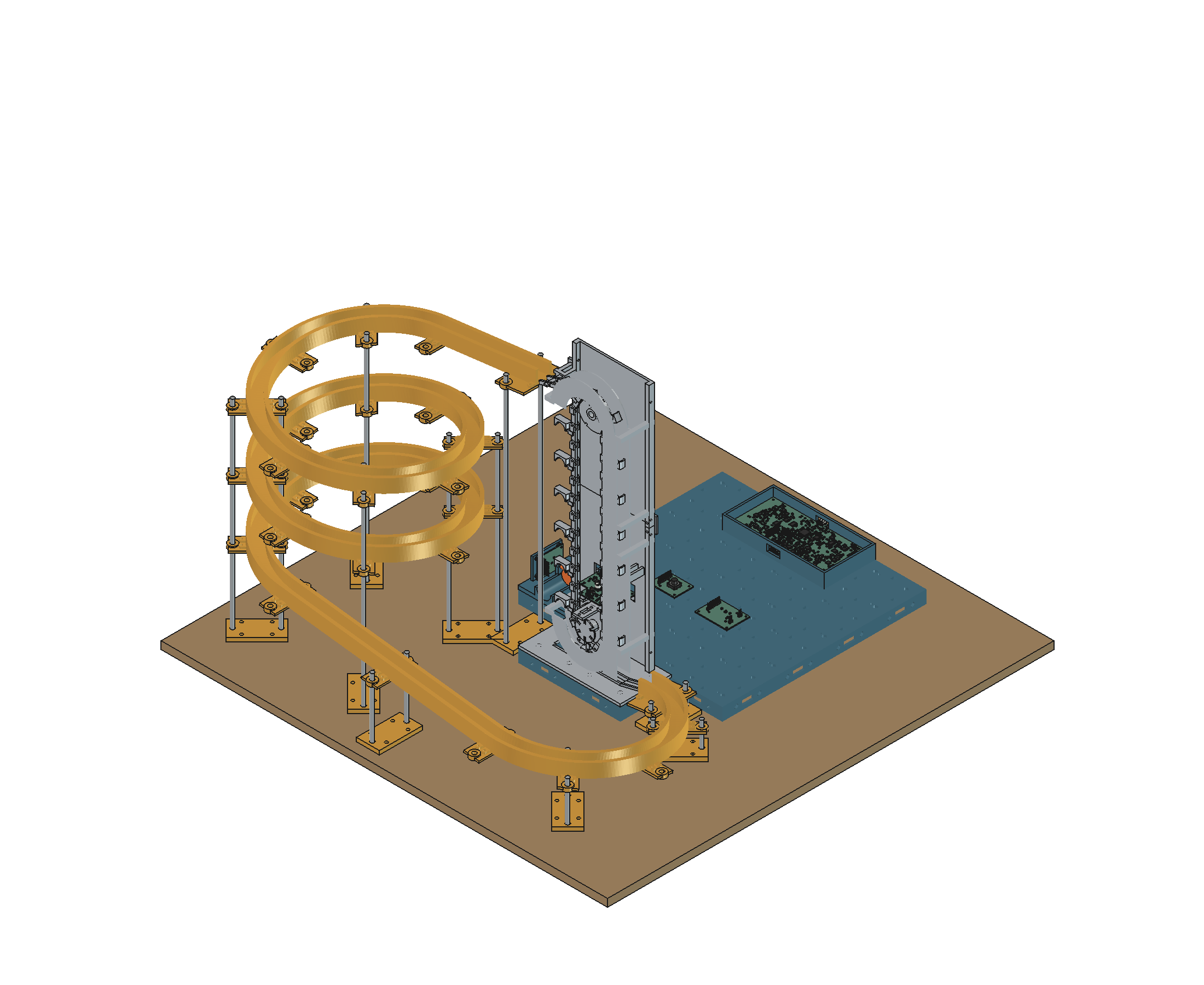
Klink is an 80x80mm magnetic tile system for programmable marble runs. V1 keeps sixteen identical intelligent tiles, a six-port Hub, removable modules and a motorized elevator for continuous circulation. Sensors, buttons, RGB LEDs and a gate let a program react to marbles and peo
Klink is an 80x80mm magnetic tile system for programmable marble runs. V1 keeps sixteen identical intelligent tiles, a six-port Hub, removable modules and a motorized elevator for continuous circulation. Sensors, buttons, RGB LEDs and a gate let a program react to marbles and people.
The design is in progress. It is not ready for main-board fabrication or Fallen Design Submission. The remaining digital work and physical qualification gates are listed below.
Flat contact test bill of materials (BOM)
6 components, 6 distinct parts — part numbers from the project's BOM.
| Qty | Part | Footprint | Refs |
|---|---|---|---|
| 1 | DEBUG_3V3_MONITOR UNQUALIFIED CONTACT TEST | Flat_contact_test_5x2mm | J1 |
| 1 | BUS_20V CH1 | TP1 | |
| 1 | TILE_20V CH2 | TP2 | |
| 1 | CH3 | TP3 | |
| 1 | CH4 | TP4 | |
| 1 | MODULE_5V CH5 | TP5 |
Flat contact test design files
The KiCad project lives in the Bruhdows/klink repository on GitHub; these links point at the commit this page was built from.
Flat contact test: common questions
How big is the Flat contact test PCB?
The Flat contact test measures 20 × 12 mm, has 2 copper layers and is 1.6 mm thick.
How many components are on the Flat contact test?
6 components, from 6 distinct parts, with part numbers taken from the project's own BOM. The full bill of materials is listed on this page.
Where can I download the Flat contact test design files?
From the Bruhdows/klink repository on GitHub, which has the KiCad layout and the BOM; the links under Design files point to each one.
Can I use the Flat contact test design in my own project?
The repository has no license, so all rights stay with Bruhdows. Use it as a reference, and ask the author before reusing the design.
More boards in klink
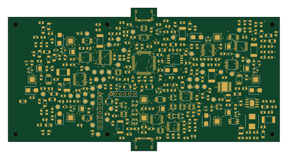 STM32
Hub
148 × 78 mm309 parts4LNo license1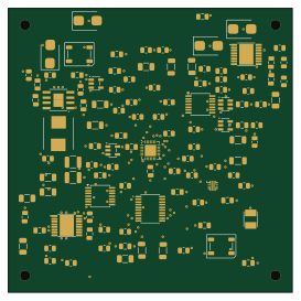 WCH CH32/CH55x
Tile
68 × 68 mm109 parts4LNo license1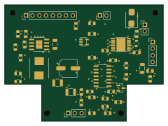 AVR/Arduino
Elevator
60 × 44 mm47 parts4LNo license1
Side flat test
40 × 12 mm15 parts2LNo license1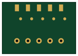
Side contact test
40 × 28 mm15 parts2LNo license1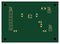
Marble sensor
50 × 36 mm11 parts2LNo license1
Spring contact test
20 × 12 mm6 parts2LNo license1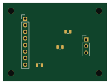
Gate
40 × 30 mm5 parts2LNo license1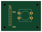
Button
40 × 30 mm4 parts2LNo license1
Similar boards
Sensor smd
scottbez1
40 × 20 mm5 parts2LApache-2.04.2k
Sensors
StuckAtPrototype
15.2 × 9 mm14 parts4LApache-2.03.8k
Microphone
Mentra-Community
5.5 × 6.1 mm6 parts2LMIT1.2k
TemperaturePCB PANEL
stuartpittaway
116 × 75.5 mm178 parts2LCC-BY-NC-4.01.1k
Pots
shanteacontrols
390 × 93 mm75 parts2LApache-2.0956
USB
52 × 12.6 mm6 parts2LApache-2.0956