
Split flap fae

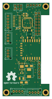
About the Split flap fae PCB
Split flap fae is an open source ESP8266 PCB design by codingcatgirl, published on GitHub under the Apache-2.0 license. It is a 2-layer board measuring 40 × 80 mm, with 39 components from 24 distinct parts.
Its main chip is the ESP-12E, from the ESP8266 family. Other key parts include the TPS5430, ULN2003A and ATMEGA328P-A. By type, the board carries 12 capacitors, 9 connectors, 8 resistors, 4 ICs, 3 diodes and 1 crystal.
It belongs with the displays & leds designs in this gallery.
From the project
Alternative drop-in replacement PCB for David Kingsman's split-flap display
This repository contains an alternative, improved, (near) drop-in replacement PCB for David Kingsman's Split-Flap Display.
Please note that due to some changes in pinout, you need to use evilscientress' improved fork of the firmware, which was specifically created along with this PCB.
- Identical PCB outline, connectors and connector positions. - Removed Arduino Nano, use its Atmega328P directly, saving cost and space. - Run the Atmega328P on 3V3, removing the need for a 5V rail and logic conversion and increasing power efficiency by using a step-down converter (TPS5430). The entire…
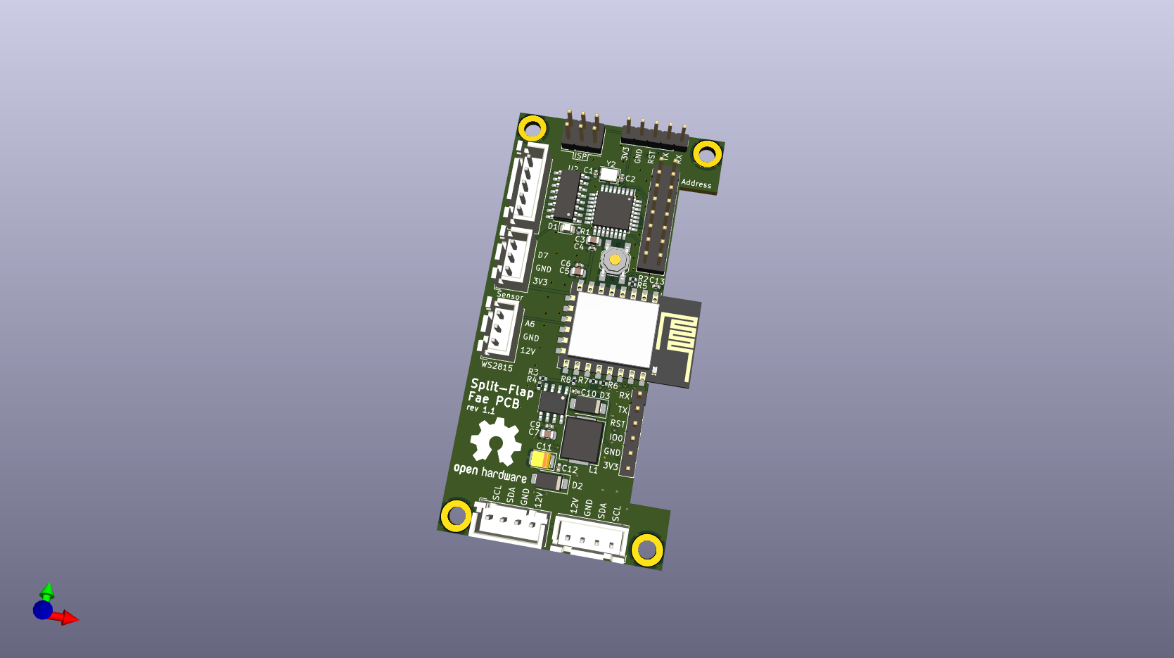
Main components on the Split flap fae
Split flap fae bill of materials (BOM)
39 components, 24 distinct parts — part numbers from the project's BOM.
| Qty | Part | Footprint | Refs |
|---|---|---|---|
| 1 | TPS5430 | SOIC-8-1EP_3.9x4.9mm_P1.27mm_EP2.514x3.2mm_ThermalVias | U1 |
| 1 | ULN2003A | SOIC-16_3.9x9.9mm_P1.27mm | U2 |
| 1 | ATMEGA328P-A ATmega328P-A | TQFP-32_7x7mm_P0.8mm | U3 |
| 1 | ESP-12E | ESP-12E | U4 |
| 1 | 16MHZ 16MHz | Crystal_SMD_3225-4Pin_3.2x2.5mm | Y2 |
| 2 | CONN_01X04_PIN Conn_01x04_Pin | JST_XH_B4B-XH-AM_1x04_P2.50mm_Vertical | J1, J2 |
| 1 | CONN_01X05_PIN Conn_01x05_Pin | JST_XH_B5B-XH-AM_1x05_P2.50mm_Vertical | J3 |
| 1 | C492425 AddressJumpers | PinHeader_2x08_P2.54mm_Vertical | J4 |
| 1 | C144394 HallSensor | JST_XH_B3B-XH-AM_1x03_P2.50mm_Vertical | J5 |
| 1 | AVR-ISP-6 | PinHeader_2x03_P2.54mm_Vertical | J6 |
| 1 | SERIAL-328P Serial-328P | PinHeader_1x05_P2.54mm_Vertical | J7 |
| 1 | SERIAL-ESP12E Serial-ESP12E | PinHeader_1x06_P2.54mm_Vertical | J8 |
| 1 | WS2815 | JST_XH_B3B-XH-AM_1x03_P2.50mm_Vertical | J9 |
| 1 | C318884 RESET | SW_SPST_SKQG_WithStem | SW1 |
| 1 | LED | LED_0805_2012Metric | D1 |
| 2 | SS54 | D_SMA | D2, D3 |
| 1 | 47UH 47uH | L_Chilisin_BMRx00060630 | L1 |
| 2 | 22PF 22pF | C_0402_1005Metric | C1, C2 |
| 3 | 10UF 10uF | C_0805_2012Metric | C3, C5, C7 |
| 6 | 100N 100n | C_0402_1005Metric | C4, C6, C9, C10, C12, C13 |
Show 4 more
| Qty | Part | Footprint | Refs |
|---|---|---|---|
| 1 | 220UF 220uF | CP_EIA-3528-21_Kemet-B | C11 |
| 1 | 220 | R_0402_1005Metric | R1 |
| 6 | 10K 10k | R_0402_1005Metric | R2, R3, R5, R6, R7, R8 |
| 1 | 5K9 5k9 | R_0402_1005Metric | R4 |
Split flap fae design files
The KiCad project lives in the codingcatgirl/split-flap-fae-pcb repository on GitHub; these links point at the commit this page was built from.
- Layoutsplitflappcb.kicad_pcb
- Schematicsplitflappcb.kicad_sch
- BOMfab/splitflappcb-bom.csv
Split flap fae: common questions
What microcontroller does the Split flap fae use?
The Split flap fae is built around the ESP-12E, from the ESP8266 family.
How big is the Split flap fae PCB?
The Split flap fae measures 40 × 80 mm, has 2 copper layers and is 1.6 mm thick.
How many components are on the Split flap fae?
39 components, from 24 distinct parts, with part numbers taken from the project's own BOM. The full bill of materials is listed on this page.
Where can I download the Split flap fae design files?
From the codingcatgirl/split-flap-fae-pcb repository on GitHub, which has the KiCad layout, the schematic and the BOM; the links under Design files point to each one.
Can I use the Split flap fae design in my own project?
Yes, under the terms of its Apache-2.0 license, which codingcatgirl chose for the repository.
Can I test firmware for the Split flap fae without the hardware?
Yes. HardLabs builds a simulation of the board from its netlist and BOM, so you can run and debug ESP8266 firmware against it before you order a PCB.
Similar boards
 ESP8266
ESP8266ControllerCircuit
stuartpittaway
75 × 30 mm20 parts2LCC-BY-NC-4.01.1k ESP8266
Duet WIFI
Duet3D
100 × 123 mm345 partsCERN-OHL-1.2257 ESP8266
RetroWiFiModem
mecparts
100 × 66.1 mm29 parts2LGPL-3.0256 ESP8266
Mideahvac dongle
reneklootwijk
20 × 48.5 mm19 parts2LNo license74 ESP8266
Single radio
AnyLeaf
37.7 × 37.7 mm43 parts4LMIT63 ESP8266
Esp8266-for uppatvind
horvathgergo
70 × 36 mm27 parts2LGPL-3.060