
Ground fill input

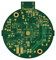
About the Ground fill input PCB
Ground fill input is an open source RP2040/RP2350 PCB design by dcuccia, published on GitHub under the MIT license. It is a 2-layer board measuring 44.5 × 48.4 mm, with 84 components from 45 distinct parts.
Its main chip is the RP2040_QFN56, from the RP2040/RP2350 family. Other key parts include the LSM6DSOXTR, W25Q16JVUXIQ TR, RT9080-3.3, MCP73831T-2ACI/OT and MAX98357A. By type, the board carries 30 capacitors, 28 resistors, 8 ICs, 5 transistors, 4 inductors and 2 crystals.
It belongs with the audio and power & battery designs in this gallery.
From the project
A software and hardware project to create a digital handbell using microcontrollers and speakers and gesture recognition
Development candidate, not a released quotation package or permission to power, fabricate or order it. This separate project continues the accepted power rework toward the owner's full JLCPCB and PCBWay PCB+PCBA quotation handoff. Current native connectivity, failures and residual nets are reported in reports/completion-review.json and its Markdown companion; filenames or an autorouter's completion message are not approval.
Main components on the Ground fill input
Ground fill input bill of materials (BOM)
84 components, 45 distinct parts — part numbers from the project's BOM.
| Qty | Part | Footprint | Refs |
|---|---|---|---|
| 1 | RP2040_QFN56 | QFN56_7MM_REDUCEDEPAD | IC1 |
| 1 | LSM6DSOXTR | LGA-14L | IC4 |
| 1 | W25Q16JVUXIQ TR W25Q16JVUXIQ TR / 2MB | Winbond_USON8_UX_2x3 | U1 |
| 1 | RT9080-3.3 | SOT23-5 | U2 |
| 1 | MCP73831T-2ACI/OT | SOT23-5 | U3 |
| 1 | MAX98357A | QFN16_3MM | U4 |
| 1 | TPS61023DRLR | SOT563 | U5 |
| 1 | BQ29700DSER | BQ29700_DSE6 | U6 |
| 1 | AO3401 | SOT23-WIDE | Q1 |
| 1 | C20917 | SOT23-WIDE | Q2 |
| 1 | DMG3415UFY | DFN2015-3_DrainPad | Q3 |
| 1 | AO3400A | SOT-23 | Q4 |
| 1 | CSD83325L | CSD83325L_YJE6 | Q5 |
| 1 | USB Type C | USB_C_CUSB31-CFM2AX-01-X | X6 |
| 1 | 12MHZ/12PF 12MHz/12pF | CRYSTAL_2.5X2 | Y1 |
| 1 | 504050-0291 | Molex_Pico-Lock_504050-0291_1x02-1MP_P1.50mm_Horizontal | J1 |
| 1 | SM02B-SRSS-TB | JST_SH_SM02B-SRSS-TB_1x02-1MP_P1.00mm_Horizontal | J2 |
| 1 | 254 Keystone 254 POS | Keystone_254_RevC | BT1 |
| 1 | 254 Keystone 254 NEG | Keystone_254_RevC | BT2 |
| 1 | ORANGE | CHIPLED_0603_NOOUTLINE | CHG0 |
Show 25 more
| Qty | Part | Footprint | Refs |
|---|---|---|---|
| 1 | 1N4148 | SOD-323_MINI | D3 |
| 1 | PMEG2020AEA | SOD-323F | D4 |
| 2 | Ferrite | 0603-NO | FB1, FB2 |
| 1 | RED | CHIPLED_0603_NOOUTLINE | L0 |
| 1 | 1uH (MPN pending) | INDUCTOR_5X5MM_TDK_VLC5045 | L1 |
| 5 | 10UF/16V 10uF/16V | 0805-NO | C1, C4, C5, C19, C20 |
| 2 | 22PF 22pF | _0402NO | C2, C3 |
| 10 | 0.1UF 0.1uF | _0402NO | C6, C7, C9, C12, C13, C14, C16, C18 +2 |
| 5 | 1UF/25V 1uF/25V | _0402NO | C8, C10, C11, C15, C17 |
| 2 | 220PF 220pF | _0402NO | C21, C22 |
| 1 | 10NF 10nF | _0402NO | C25 |
| 3 | 22UF 22uF | 0805-NO | C26, C27, C28 |
| 1 | 220pF (DNP) | _0402NO | C29 |
| 1 | GRM155R71C104KA88D 100n 16V X7R | _0402NO | C30 |
| 10 | 10K | _0402NO | R1, R2, R3, R4, R5, R7, R14, R15 +2 |
| 3 | 1K | _0402NO | R6, R11, R22 |
| 3 | 5.1K | _0402NO | R8, R12, R13 |
| 2 | 22 ohm | _0402NO | R9, R10 |
| 3 | 100K | _0402NO | R16, R17, R24 |
| 1 | 4.7K | _0402NO | R20 |
| 1 | 732K | _0402NO | R23 |
| 1 | RC0402FR-07330RL 330R | _0402NO | R25 |
| 1 | RC0402FR-072K2L 2.2k | _0402NO | R26 |
| 1 | ERJ-6BWFR033V 33m 1% 0.5W | ERJ6BW_0805 | R27 |
| 2 | RC0402FR-075M1L 5.1M gate discharge | _0402NO | R28, R29 |
Ground fill input design files
The KiCad project lives in the dcuccia/digital-handbell repository on GitHub; these links point at the commit this page was built from.
Ground fill input: common questions
What microcontroller does the Ground fill input use?
The Ground fill input is built around the RP2040_QFN56, from the RP2040/RP2350 family.
How big is the Ground fill input PCB?
The Ground fill input measures 44.5 × 48.4 mm, has 2 copper layers and is 1.6 mm thick.
How many components are on the Ground fill input?
84 components, from 45 distinct parts, with part numbers taken from the project's own BOM. The full bill of materials is listed on this page.
Where can I download the Ground fill input design files?
From the dcuccia/digital-handbell repository on GitHub, which has the KiCad layout and the BOM; the links under Design files point to each one.
Can I use the Ground fill input design in my own project?
Yes, under the terms of its MIT license, which dcuccia chose for the repository.
Can I test firmware for the Ground fill input without the hardware?
Yes. HardLabs builds a simulation of the board from its netlist and BOM, so you can run and debug RP2040/RP2350 firmware against it before you order a PCB.
More boards in digital-handbell
 RP2040/RP2350
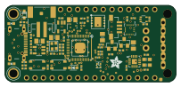
Adafruit Feather RP2040 Prop-Maker
50.8 × 22.9 mm160 parts2LMIT0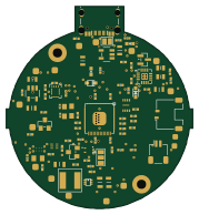 RP2040/RP2350
Imu fanout method staged
44.5 × 48.4 mm84 parts4LMIT0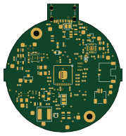 RP2040/RP2350
Imu cleanup staged
44.5 × 48.4 mm84 parts4LMIT0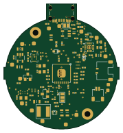 RP2040/RP2350
C23-usbboot staged
44.5 × 48.4 mm84 parts4LMIT0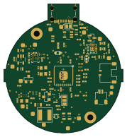 RP2040/RP2350
Imu coupled working
44.5 × 48.4 mm84 parts4LMIT0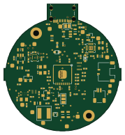 RP2040/RP2350
Mcu vcore source cell rejected
44.5 × 48.4 mm84 parts4LMIT0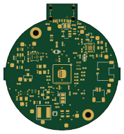 RP2040/RP2350
Mcu east ground staged
44.5 × 48.4 mm84 parts4LMIT0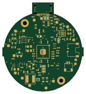 RP2040/RP2350
Imu electrical filled
44.5 × 48.4 mm84 parts4LMIT0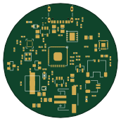 RP2040/RP2350
Handbell 0.2 - UNROUTED PLACEMENT ONLY
43 × 43 mm75 parts2LMIT0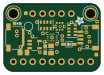
Adafruit LSM6DSOX
25.4 × 17.8 mm19 parts2LMIT0 RP2040/RP2350
Adafruit TPS61023
11.4 × 17.8 mm11 parts2LMIT0
Similar boards
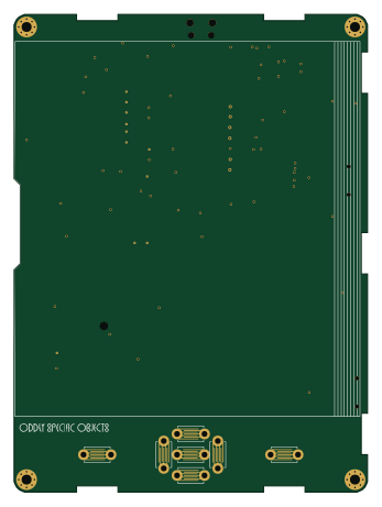 RP2040/RP2350
Open Book Abridged Edition
joeycastillo
85 × 115 mm29 parts2LCC-BY-SA-4.08.1k RP2040/RP2350
Corne
foostan
277.2 × 107.5 mm164 parts2LCC-BY-4.07.7k RP2040/RP2350
Corne
277.2 × 107.5 mm164 parts2LCC-BY-4.07.7k RP2040/RP2350
LogicAnalyzer
gusmanb
57 × 55.2 mm6 parts2LGPL-3.05.0k RP2040/RP2350
Jitx design
55.5 × 65 mm26 parts4LGPL-3.05.0k RP2040/RP2350
Pro V2
kata0510
290.1 × 130 mm270 parts2LMIT2.3k