
VIA PLCC2DIP

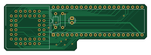
About the VIA PLCC2DIP PCB
VIA PLCC2DIP is an open source PCB design by demik, published on GitHub under the CERN-OHL-P-2.0 license. It is a 2-layer board measuring 77.5 × 25.4 mm, with 5 components from 5 distinct parts.
Other key parts include the LF347. By type, the board carries 2 ICs, 1 diode, 1 capacitor and 1 resistor.
It belongs with the retro computing designs in this gallery.
From the project
Development ressources for Old World Macintosh (68k and NuBus PPC) and a few related things…
Pins labelled on top of the PCB. Power LED as extra
Main components on the VIA PLCC2DIP
VIA PLCC2DIP bill of materials (BOM)
5 components, 5 distinct parts — part numbers from the project's BOM.
| Qty | Part | Footprint | Refs |
|---|---|---|---|
| 1 | LF347 WD65C22 | DIP-40_W15.24mm | U1 |
| 1 | LF347 WD65C22 | PLCC-44_THT-Socket | U2 |
| 1 | LED | LED_D3.0mm | D1 |
| 1 | 100NF C | C_Axial_L3.8mm_D2.6mm_P7.50mm_Horizontal | C1 |
| 1 | 330 | R_Axial_DIN0207_L6.3mm_D2.5mm_P7.62mm_Horizontal | R1 |
VIA PLCC2DIP design files
The KiCad project lives in the demik/oldworld repository on GitHub; these links point at the commit this page was built from.
VIA PLCC2DIP: common questions
How big is the VIA PLCC2DIP PCB?
The VIA PLCC2DIP measures 77.5 × 25.4 mm, has 2 copper layers and is 1.6 mm thick.
How many components are on the VIA PLCC2DIP?
5 components, from 5 distinct parts, with part numbers taken from the project's own BOM. The full bill of materials is listed on this page.
Where can I download the VIA PLCC2DIP design files?
From the demik/oldworld repository on GitHub, which has the KiCad layout, the schematic and the BOM; the links under Design files point to each one.
Can I use the VIA PLCC2DIP design in my own project?
Yes, under the terms of its CERN-OHL-P-2.0 license, which demik chose for the repository.
More boards in oldworld
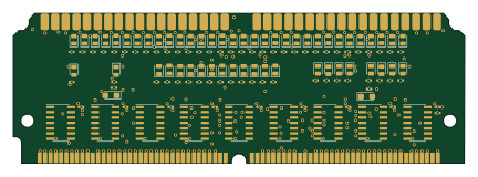
SIMM72BL
108 × 35.8 mm133 parts4LCERN-OHL-P-2.027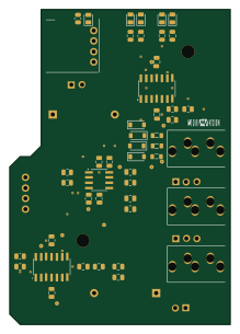
NUBUSPAS16-DB
53.3 × 76.2 mm54 parts2LCERN-OHL-P-2.027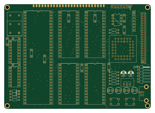
68k nano single board computer
127 × 90.8 mm49 parts2LCERN-OHL-P-2.027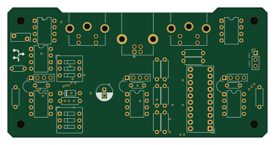 PIC
PICADBDB
100 × 50 mm34 parts2LCERN-OHL-P-2.027- schematic only · 33 parts
PICDB
33 parts2LCERN-OHL-P-2.027 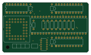
VIA Plus
77.5 × 44.7 mm18 parts4LCERN-OHL-P-2.027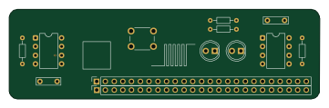 AVR/Arduino
68k nano watchdog
90.2 × 26 mm13 parts2LCERN-OHL-P-2.027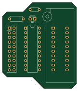
PAL16R LART
40.6 × 47 mm6 parts2LCERN-OHL-P-2.027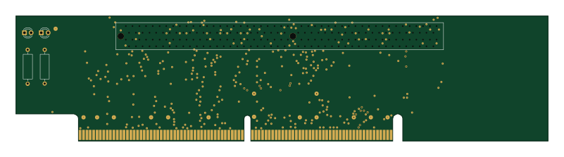
PowerMac 6100 HPV Riser
200 × 47 mm6 parts2LCERN-OHL-P-2.027
PB5xx ATXCPU
25 × 35 mm5 parts2LCERN-OHL-P-2.027
PB5xx Floppy Adapter
20 × 60 mm3 parts2LCERN-OHL-P-2.027
Similar boards
OpenTendo
Redherring32
196.3 × 118.7 mm93 parts2LTAPR-OHL-1.0850
24pin flex interposer
Wren6991
29 × 32 mm3 parts2LNo license508
Sram dev board
50 × 50 mm12 parts2LNo license508
GB-BRK-SLOT-A
Gekkio
81 × 80 mm20 parts2LCC-BY-4.0376
GB-BRK-SLOT-B
81 × 80 mm20 parts2LCC-BY-4.0376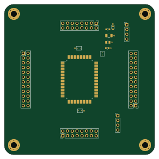
GB-BRK-CPU-G2
80 × 80 mm12 parts2LCC-BY-4.0376