
Audcalc

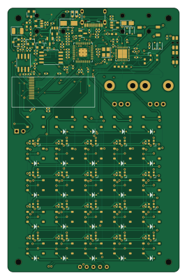
About the Audcalc PCB
Audcalc is an open source RP2040/RP2350 PCB design by jonbro, published on GitHub under the MIT license. It is a 4-layer board measuring 65 × 100 mm, with 214 components from 58 distinct parts.
Its main chip is the RP2040, from the RP2040/RP2350 family. Other key parts include the W25Q32JVSS, TLV320AIC3204, WMM7037AT2_mic, HCPL-0631 and MCP73831T-2ATI_OT. By type, the board carries 66 capacitors, 52 diodes, 35 resistors, 27 switches, 9 ICs and 9 jumpers.
It belongs with the audio designs in this gallery.
From the project
pocket sized groovebox
I'm happy with this, but its not 100% feature complete on the firmware side. Its really neat though, and I think you'll like it.
- RP2040 - 1/8in audio i/o - onboard mic - 104mm x 68mm x 14mm
The bom is contained within the Hardware kicad project, ready for assembly via jlcpcb. There are several additional items that must be sourced and handsoldered:
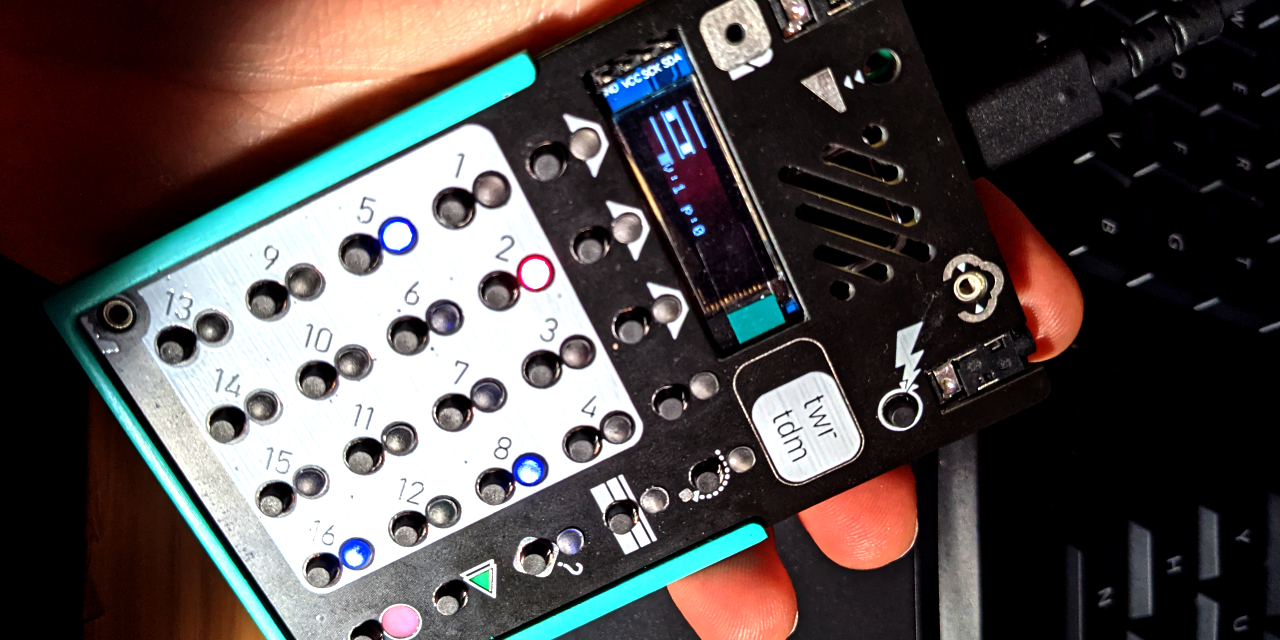
Main components on the Audcalc
Audcalc bill of materials (BOM)
214 components, 58 distinct parts.
| Qty | Part | Footprint | Refs |
|---|---|---|---|
| 1 | W25Q32JVSS | SOIJ-8_5.3x5.3mm_Pitch1.27mm | U1 |
| 1 | RP2040 | RP2040-QFN-56 | U2 |
| 1 | TLV320AIC3204 | QFN-32-1EP_5x5mm_Pitch0.5mm | U3 |
| 1 | WMM7037AT2_mic | LGA-4 (3x3.8) | U4 |
| 1 | HCPL-0631 | SOIC-8_3.9x4.9mm_P1.27mm | U5 |
| 1 | MCP73831T-2ATI_OT | SOT-23-5 | U6 |
| 1 | LM4040DBZ-2.5 | SOT-23 | U7 |
| 2 | ME6211C | SOT-23-5 | U9, U11 |
| 1 | DMG2305UX-13 | SOT-23-3 | Q1 |
| 1 | Q_PMOS_GSD | SOT-23 | Q2 |
| 2 | Q_NMOS_GSD | SOT-23 | Q3, Q4 |
| 1 | Crystal_GND24 | Crystal_SMD_3225-4pin_3.2x2.5mm | Y1 |
| 1 | picoprobe_debug | pico debug header | J1 |
| 1 | USB_C_Receptacle_USB2.0 | USB-C_SMD-TYPE-C-31-M-12 | J2 |
| 1 | line_in | HRO-PJ-327C-A | J3 |
| 1 | headphone_out | HRO-PJ-327C-A | J4 |
| 1 | midi_in | HRO-PJ-327C-A | J5 |
| 1 | midi_out | HRO-PJ-327C-A | J6 |
| 1 | battery | JST_PH_S2B-PH-SM4-TB_02x2.00mm_Angled | J7 |
| 1 | Conn_01x02_Female | PinHeader_1x02_P2.54mm_Vertical | J8 |
Show 38 more
| Qty | Part | Footprint | Refs |
|---|---|---|---|
| 2 | SolderJumper_2_Open | SolderJumper-2_P1.3mm_Open_RoundedPad1.0x1.5mm | JP1, JP2 |
| 7 | SolderJumper_2_Bridged | SolderJumper-2_P1.3mm_Bridged_Pad1.0x1.5mm | JP3, JP4, JP5, JP6, JP7, JP8, JP14 |
| 2 | R_POT_US | Potentiometer_Alps_RK09K_Horizontal | RV1, RV2 |
| 25 | spst_4_pin_internal | ts1187 | SW1, SW2, SW3, SW4, SW5, SW6, SW7, SW8 +17 |
| 2 | spst_4_pin_internal_side | SKSCLDE010 | SW26, SW27 |
| 1 | 128x32OLED | oled_ssd1306_14pin_91 | LCD1 |
| 1 | BAT54C | SOT-23 | D1 |
| 1 | LEDYellow | LED_0603 | D2 |
| 4 | D_Zener | D_SOD-323F | D3, D4, D5, D26 |
| 20 | WS2812C-v1 | ws2812b-2020-lightpipe | D6, D7, D8, D9, D10, D11, D12, D13 +12 |
| 24 | D | D_SOD-323F_less_silk | D27, D28, D29, D30, D31, D32, D33, D34 +16 |
| 1 | D_Schottky | D_SMA | D53 |
| 1 | LED | LED_0603 | D54 |
| 29 | 1u | C_0402_1005Metric | C1, C6, C7, C8, C9, C10, C11, C12 +21 |
| 14 | 100n | C_0402_1005Metric | C2, C3, C5, C26, C27, C28, C29, C30 +6 |
| 11 | 10u | C_0402_1005Metric | C4, C36, C38, C42, C43, C46, C50, C55 +3 |
| 2 | 30p | C_0402_1005Metric | C35, C37 |
| 4 | .47u | C_0603_nosilk | C39, C44, C45, C47 |
| 2 | 47uf | C_1206 | C48, C49 |
| 1 | 10u(tant) | CP_Tantalum_Case-A_EIA-3216-18_Reflow | C58 |
| 1 | 10n | C_0402_1005Metric | C59 |
| 1 | 100u | CP_EIA-3528-21_Kemet-B | C65 |
| 1 | 2u2 | C_0402_1005Metric | C66 |
| 2 | 27.4 | R_0402_1005Metric_nosilk | R1, R2 |
| 5 | 10k | R_0402_1005Metric_nosilk | R3, R9, R14, R24, R30 |
| 2 | 3.3k | R_0402_1005Metric_nosilk | R4, R5 |
| 4 | 1k | R_0402_1005Metric_nosilk | R6, R7, R17, R31 |
| 3 | 100k | R_0402_1005Metric_nosilk | R8, R18, R25 |
| 3 | 220 | R_0402_1005Metric_nosilk | R10, R11, R21 |
| 3 | 33 | R_0402_1005Metric_nosilk | R12, R34, R35 |
| 1 | 10 | R_0402_1005Metric_nosilk | R13 |
| 1 | 330k | R_0402_1005Metric_nosilk | R15 |
| 1 | 4.7k | R_0402_1005Metric_nosilk | R16 |
| 3 | 5.1k | R_0402_1005Metric_nosilk | R19, R20, R23 |
| 2 | 330 | R_0402_1005Metric_nosilk | R22, R26 |
| 2 | 1m | R_0402_1005Metric_nosilk | R27, R28 |
| 1 | 750k | C_0603_nosilk | R29 |
| 2 | 100 | R_0402_1005Metric | R32, R33 |
Audcalc design files
The KiCad project lives in the jonbro/Audcalc repository on GitHub; these links point at the commit this page was built from.
Audcalc: common questions
What microcontroller does the Audcalc use?
The Audcalc is built around the RP2040, from the RP2040/RP2350 family.
How big is the Audcalc PCB?
The Audcalc measures 65 × 100 mm, has 4 copper layers and is 1.6 mm thick.
How many components are on the Audcalc?
214 components, from 58 distinct parts. The full bill of materials is listed on this page.
Where can I download the Audcalc design files?
From the jonbro/Audcalc repository on GitHub, which has the KiCad layout and the schematic; the links under Design files point to each one.
Can I use the Audcalc design in my own project?
Yes, under the terms of its MIT license, which jonbro chose for the repository.
Can I test firmware for the Audcalc without the hardware?
Yes. HardLabs builds a simulation of the board from its netlist and BOM, so you can run and debug RP2040/RP2350 firmware against it before you order a PCB.
Similar boards
 RP2040/RP2350
Open Book Abridged Edition
joeycastillo
85 × 115 mm29 parts2LCC-BY-SA-4.08.1k RP2040/RP2350
Corne
foostan
277.2 × 107.5 mm164 parts2LCC-BY-4.07.7k RP2040/RP2350
Corne
277.2 × 107.5 mm164 parts2LCC-BY-4.07.7k RP2040/RP2350
LogicAnalyzer
gusmanb
57 × 55.2 mm6 parts2LGPL-3.05.0k RP2040/RP2350
Jitx design
55.5 × 65 mm26 parts4LGPL-3.05.0k RP2040/RP2350
Pro V2
kata0510
290.1 × 130 mm270 parts2LMIT2.3k